Facebook
 Google
 GitHub
 Linkedin
Discrete Semiconductor Devices and Circuits
Electrical Conduction in Semiconductors
17 questions By Tony R. Kuphaldt
-
Question 16 of 17
Draw the approximate locations of the Fermi levels in these three energy level diagrams:
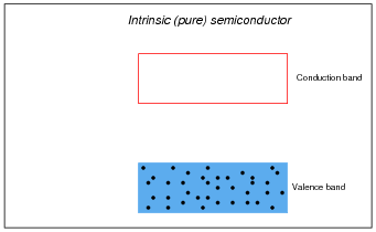
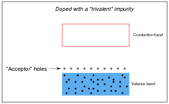

Reveal answer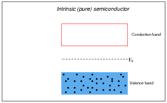

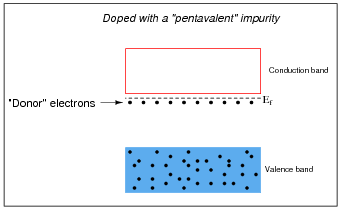
Notes:Note how much the Fermi level is affected by the addition of dopants to an otherwise pure semiconducting material. Understanding this effect is critical to the understanding of PN semiconductor junctions.
-
Question 17 of 17
A fascinating experiment carried out by J. R. Hayes and W. Shockley in the early 1950’s involved a bar of N-doped germanium with two metal point contacts labeled Ë” and “C,” for “Emitter” and “Collector,” respectively:
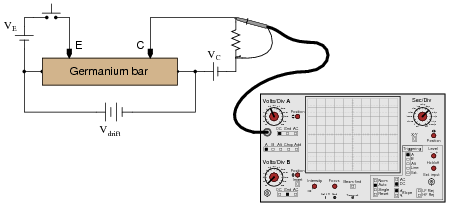
Upon actuating the switch, two distinct pulses were noted on the oscilloscope display:
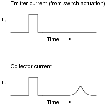
With less drift voltage (Vdrift) applied across the length of the bar, the second pulse was seen to be further delayed and more diffused:

The instantaneous effect of the first pulse (precisely timed with the closure of the switch) is not the most interesting facet of this experiment. Rather, the second (delayed) pulse is. Explain what caused this second pulse, and why its shape depended on Vdrift.
Reveal answerThe second pulse arose from a “cloud” of holes injected into the N-type germanium bar from the point contact emitter. Vdrift provided an electric field to make these holes “drift” from left to right through the bar, where they were eventually detected by the collector point contact.
Notes:This tidbit of semiconductor history was found in Electronics for Scientists and Engineers
, by R. Ralph Benedict, on pages 113 and 114. Like many other engineering textbooks of the 1950’s and 1960’s, this publication is at once a treasure trove of technical information and a model of clarity. I only wish the technician-level textbooks of today could be so lucid as the engineering-level textbooks of decades ago. As you might have guessed, I enjoy haunting used book stores in search of vintage engineering texts!