Facebook
 Google
 GitHub
 Linkedin
Analog Integrated Circuits
Inverting and Noninverting OpAmp Voltage Amplifier Circuits
41 questions By Tony R. Kuphaldt
-
Question 40 of 41
The junction between the two resistors and the inverting input of the operational amplifier is often referred to as a virtual ground, the voltage between it and ground being (almost) zero over a wide range of circuit conditions:
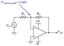
If the operational amplifier is driven into saturation, though, the “virtual ground” will no longer be at ground potential. Explain why this is, and what condition(s) may cause this to happen.
Hint: analyze all currents and voltage drops in the following circuit, assuming an opamp with the ability to swing its output voltage rail-to-rail.
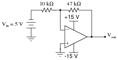
Reveal answerAny input signal causing the operational amplifier to try to output a voltage beyond either of its supply rails will cause the “virtual ground” node to deviate substantially from ground potential.
Notes:Before students can answer this question, they must understand what saturation means with regard to an operational amplifier. This is where the “hint” scenario comes into play. Students failing to grasp this concept will calculate the voltage drops and currents in the “hint” circuit according to standard procedures and assumptions, and arrive at an output voltage well in excess of 15 volts. Resolving this paradox will lead to insight, and hopefully to a more realistic set of calculations.
-
Question 41 of 41
The same problem of input bias current affecting the precision of opamp voltage buffer circuits also affects non-inverting opamp voltage amplifier circuits:
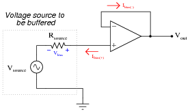
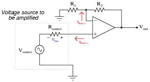
To fix this problem in the voltage buffer circuit, we added a “compensating” resistor:
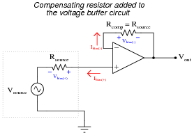
To fix the same problem in the non non-inverting voltage amplifier circuit, we must carefully choose resistors R1 and R2 so that their parallel equivalent equals the source resistance:
R1 || R2 = Rsource Of course, we must also be sure the values of R1 and R2 are such that the voltage gain of the circuit is what we want it to be.
Determine values for R1 and R2 to give a voltage gain of 7 while compensating for a source resistance of 1.45 kΩ.
Reveal answerR1 = 1.692 kΩ R2 = 10.15 kΩ
Notes:Students must apply algebra to solve for the values of these two resistances. The solution is an application of algebraic substitution, and it is worthwhile to examine and discuss together in class.
Discuss how this solution to the bias current problem is a practical application of Thévenin’s theorem: looking at the two voltage divider resistors as a network that may be Thévenized to serve as a compensating resistance as well as a voltage divider for the necessary circuit gain.