Facebook
 Google
 GitHub
 Linkedin
Common Antenna Integration Challenges and How to Handle Them
The design of RF systems requires engineers to face complex challenges. Learn how automated tools augmented with AI are becoming available to help with this.
Getting an RF system to work in practice demands detailed consideration of design theory and external factors unique to the application and operating environment, to build a system that is robust, reliable, and mass-producible.
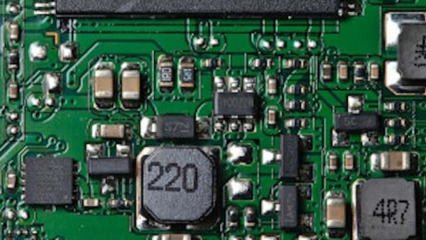
Objects such as electronic components or a battery close to the RF circuitry, or PCB planes and traces, cables, metal parts, or other bulky mechanical components, can influence signals and impact the performance. Making allowances for these to ensure acceptable performance, also considering any effects of the environment where the equipment is intended to be used, can demand hard-earned experience and engineering intuition. Achieving everything within a constrained footprint, which may be necessary to fit into a tight space or comply with a defined form factor, adds to the difficulties.
Experience can help anticipate some of the issues and minimize their effects by design. However, some amount of trial and error is usually involved and every extra design iteration needed to correct these errors adds cost to the project and could delay market entry.
Wireless Gaming Mouse Design Example
To illustrate the challenges that can be encountered, engineers at Ignion, a company that provides antennas and software tools to automate selection and design-in, focused on the design of a wireless gaming mouse (Figure 1).
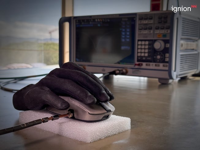
Figure 1. The gaming mouse must deliver superior performance within a comfortable, usable form factor.
In this application, high receiver sensitivity and transmitter performance are needed to ensure satisfying gameplay and minimum latency while the radio subsystem must coexist with features above and beyond those of an ordinary desktop mouse. On the other hand, usability demands that the form factor should be the same.
Antenna Selection and Integration
To design the Bluetooth radio subsystem, engineers must keep in mind the positions of the circuit board, switches, battery compartment and any metal parts, as well as the properties of the enclosure material, to ensure the radio performance will comply with Bluetooth standards.
A suitable antenna is needed, recognizing that the choices are constrained by the size limits of the mouse. Antenna selection always demands a compromise between size and performance. The antenna selection process can be labour intensive, studying the datasheets of many candidate parts in detail.
Ensuring maximum power transfer requires matching the impedance of the antenna to the transmission line, typically 50 Ω. This is not universally known and is often overlooked. Mismatches can cause signal reflections, leading to power loss and distortion. The design of the antenna feeding line connection is critical, including location and dimensions.
The impedance-matching through filtering components between the antenna and RF chipset must be selected, and their layout and optimum connections determined, including PCB pad sizes, track lengths, and gap widths.
The antenna clearance area must be free of any conductive layers or metallic components to prevent unwanted interactions from detuning the antenna. Ensuring adequate clearance within the constraints of the overall form factor and needed PCB size can be difficult, demanding careful study and compromises based on experience.
Nearby objects in the RF environment such as the enclosure and other materials can affect antenna impedance as well as radiation patterns, causing signal reflections and multipath effects that lead to distortion and fading. Sometimes the ideal design or layout is not possible due to other constraints.
Cutting the Cost of Iteration
When the design work is completed, anticipating the effects of all these issues as thoroughly as possible, the typical next step is to build a prototype and start testing under simulated real-world conditions. This testing can be expected to highlight some deficiencies that may require redesign.
This could include repositioning components, adjusting the PCB layout or trace lengths, optimizing pad sizes, fine-tuning any filters, or introducing shielding or suppression. By this stage, a significant investment in time and hardware will have been made, which must be repeated with each iteration until the desired performance is achieved.
Software tools are available that can help improve designs before committing to any hardware. Ignion’s antenna integration platform, Oxion, prioritizes antenna selection and design-in, with its Virtual Antenna technology (Figure 2). This provides a range of chip antennas, optimised for popular wireless technologies and applications such as asset tracking and IoT devices, and accurately modelled in software.
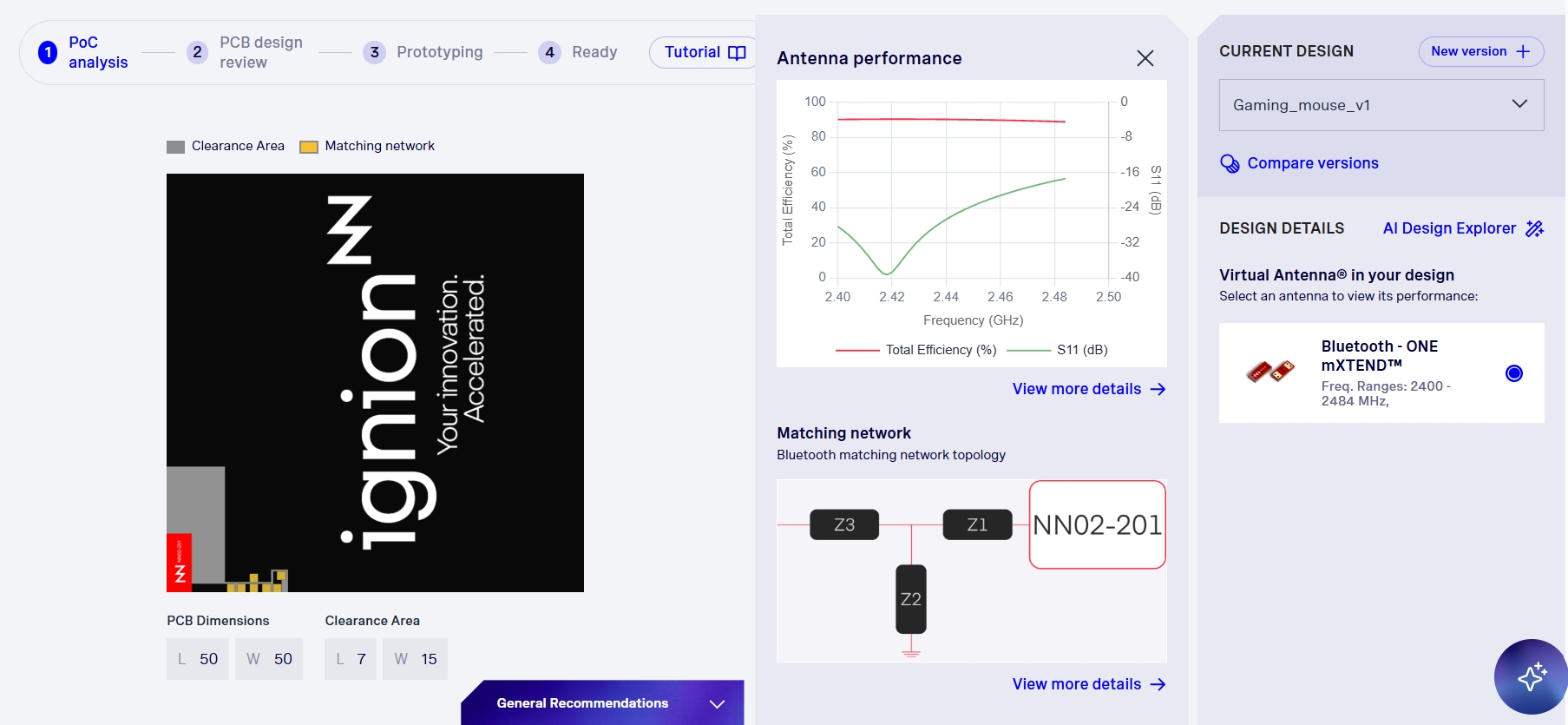
Figure 2. The RF system performance and antenna integration can be assessed in detail at PoC. (Click on image to enlarge)
Oxion helps with antenna selection and enables engineers to quickly evaluate the performance in the digital world and quickly refine their designs through rapid iteration enabled by the platform’s proprietary machine-learning model. Comparing the performance of different iterations (Figure 3) shows how the design is improving and helps accelerate the project.
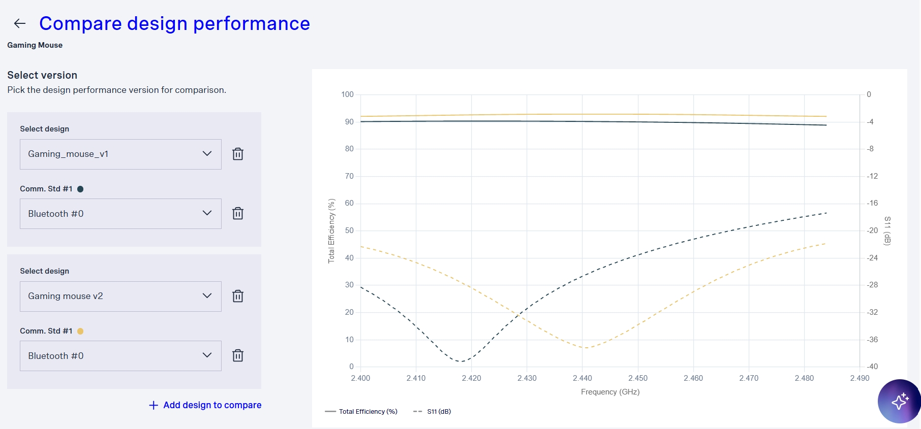
Figure 3. Graphical performance comparisons help engineers find the way forward. (Click on image to enlarge)
The latest release, Oxion 2.0, automates more of the design process by adding PCB gerber review tools to existing features such as the AI Design Explorer provided in version 1.0. AI Design Explorer is the interactive tool that enables rapid iteration and assesses the real-time performance impact of design changes.
It draws on the experience of thousands of project examples to help optimize the antenna design including placement, dimensions, and clearance. The PCB gerber review (Figure 4) supports a wide variety of use cases and automates checking of the design for compliance with guidelines and requirements appropriate to these, including validating the antenna integration.
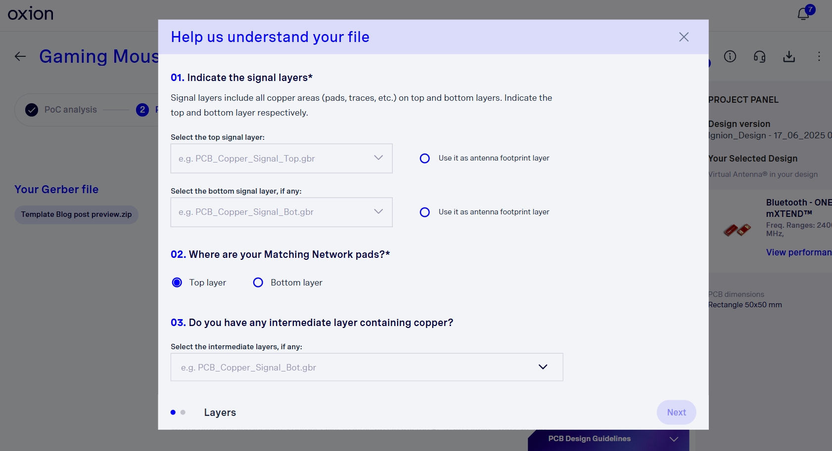
Figure 4. The PCB gerber review helps ensure all engineering issues are considered properly (Click on image to enlarge).
Proper Care Before Prototyping
After reviewing the design using a tool like this, the project can move forward into the prototype phase more confidently and expect to encounter fewer issues, if any, that need attention. In complex cases, or if real-world support is needed, Ignion can provide further services including the Matching Network Service that helps optimize the antenna performance in the real world to ensure the design functions as intended beyond simulations.
In addition, Ignion’s Peripherals Impact Consultancy helps understand how external factors such as the human body or nearby components may influence antenna behaviour. There is also Pre-Certification Analysis to help prepare for official testing at a test house approved by the appropriate certification body.
When the design work is completed, the platform creates the bill of materials (BOM) by referring to live component inventory at selected distributors. This simplifies ordering a small quantity of components for building a prototype to take into the test chamber.
Using a vector network analyser (VNA), the most important parameters to check are the antenna impedance and reflection coefficient. In the wireless mouse project, the enclosure or the presence of the user’s hand (Figure 5)—as well as parts such as batteries or metallic components close to the antenna—can cause detuning. The VNA results can guide any needed adjustment of the matching-network components to restore the antenna performance, ultimately helping achieve the desired user experience.

Figure 5. The first prototype should deliver close-to expected performance, using results from the test chamber to guide any adjustments.
Deep Expertise Applied Early
The RF system design journey is complex and calls for deep expertise from as early as the proof-of-concept stage. Taking proper care to ensure that the antenna selection, position, and connections including pads, feeding line, and matching network are correct can pay dividends later.
Digital tools have automated these aspects and are now introducing more AI in the engineering process to support engineers and guide their decisions. Automating the PCB design review means better designs go forward to prototyping. It all saves time and cost in the development lab and in the test house, ensuring faster certification and market entry.
All images used courtesy of Ignion.
Related Content