 Facebook
 Google
 GitHub
 Linkedin
Implementing an Electronic Leveling Tool
While it can be challenging to design electronic versions of precision tools, in this Industry Article we design an electronic level that matches the features of a conventional tool.
While it can be challenging to design electronic versions of precision tools, in this Industry Article we design an electronic level that matches the features of a conventional tool.
First, we will present a brief history of leveling tools. Then, we will describe the circuitry required to manage the signal received from an accelerometer. We will then discuss the internal design for a Configurable Mixed-signal Integrated Circuit (CMIC) which performs the main functions of the electronic tool. We chose to use the GreenPAK SLG46120V for this app note thanks to its size and flexibility. Finally, we will show our visual and audible interface.
History and Secrets of the Leveling Tool
A level is a tool designed to tell the user whether a surface is straight in the horizontal (also known as level) or vertical (also known as plumb) directions.
This simple piece of information is vital to brickwork, metal work, and carpentry. The design has essentially stayed unchanged for decades – a basic level contains a glass vial that is completely filled with liquid except for a small bubble. Due to the combined action of gravity and density differences, the bubble always moves to the highest point of the vial as gravity acts on the liquid inside the vial’s curved surface.
.png)
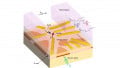
Figure 1. Exaggerated glass vial and bubble behavior.
Figure 1 illustrates an exaggeration of the glass vial which highlights how it works. Figure 1(a) shows the bubble is centered when the vial is perfectly horizontal. In Figure 1(b), the bubble migrates to the highest point when the vial is rotated. Notice that the old position marked as the faded bubble has a lower height. Since the bubble is less dense, it always floats toward the top of the curved vial surface.
Leveling Tool Design
Despite the simple mechanism, it is critical that the leveling tool performs with very high precision. The sensitivity is an important specification for a level, as it plays a big part in determining the overall accuracy of the device. The sensitive nature of a level is the change of angle or gradient required to move the bubble by a set distance. If the vial has graduated divisions, then the sensitivity refers to the angle or gradient change needed to move the bubble by one of these divisions.
The sensitivity is directly related to the radius of the curvature of the vial. The longer the radius, the more sensitive the vial will be, and vice versa. For this application note, we will use a simple bubble level as a reference. These simple levels do not come with a sensitivity specification, but it is possible to roughly measure its sensitivity by using a ruler and a caliper. Figure 2(a) shows the real bubble level tool used as a reference in this application note.

Figure 2. Actual level and rough sensitivity measurement scheme.
For the measurement, we used a 31cm long ruler and placed a general level over it. Figure 2(b), shows the ruler touching the surface at one end while raising the other. We used the caliper to measure the height at the raised side. The bubble rests in the middle of the vial when the ruler is parallel to a plane surface. In this case, the value of α is zero. Then, we raised one end of the ruler until it reached the first black mark and recorded the height, which is the variable ‘b’ denoted in Figure 2(b). The sensitivity is calculated using the following formula:

Thus, the sensitivity between the two black marks is 3.14°. Our goal is to design an electronic level that is at least as good as the bubble level.
Next, we need to discuss the electronics used to create the electronic level which has an impact on the sensitivity. The sensitivity relates directly to the features of the gravity sensor. In this application note, we used the NXP accelerometer MMA7260QT(PDF). This device features signal conditioning, a 1-pole low pass filter, temperature compensation and the ability to select between four sensitivity settings. The average current consumption of the device is 500µA during operation, but it drops down to 3µA after entering sleep mode.
The NXP accelerometer’s VDD requirements are 2.2 V-3.6 V since this is considered a low power application. The maximum sensitivity is 800 mV/g at 1.5 g, which is its default configuration. The output value of the acceleration variable is an analog voltage, and when the designer is interested only on the gravity vector, the output voltage can be described according to the following formula:

• Vy(α) is the accelerometer voltage output.
• α is the angle with respect to the g.
• Vs is the sensitivity voltage in V/g.
| α | VV(α) |
| -1.57º | -0.0219 V |
| -0.7850º | -0.0110 V |
| 0º | 0 V |
| 0.7850º | 0.0110 V |
| 1.57º | 0.0219 |
The sensitivity will scale linearly with the supply voltage. This means that as the supply voltage linearly increases, the same happens to the sensitivity and offset. Table 1 shows values for values of inside the range of the sensitivity measured before.

Figure 3. Accelerometer output when it is fully rotated.
Figure 3 illustrates the effect of rotating the accelerometer in the angle range of -360 < α < 360. Values very close to zero are nearly linear, which is very desirable in our design.
Solution Architecture
This section of the app note will describe the building blocks of the electronic leveling tool and detail how the circuit is constructed.
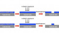
We start with Figure 4, which shows a complete block diagram of the system. The design has two main sections: Signal Conditioning and CMIC Core. The tan box contains the blocks that generate and condition the signal, and the green box contains the GreenPAK integrated circuit and its support parts as RC timing network, audio driver, and a visual indicator. The GreenPAK SLG46120V IC was chosen to perform multiple functions, including an oscillator, sound driver, and LED array.

Figure 4. System block diagram.
External Circuits
Figure 5(a) shows the module board and Figure 5(b) shows the pinout of the Accelerometer sensor.

Figure 5. Accelerometer module and pinout.
Block 1 is composed of an off-the-shelf accelerometer sensor module, which performs the acquisition of the gravity vector projection measure in its axis. The output is an analog signal in which the voltage is proportional to the projection of the gravity vector in one of three axes.
The Sel1 and Sel2 pins are two input pins that allow the user select the sensitivity of the accelerometer. By leaving SEL1 and SEL2 unconnected, the default sensitivity is 1.5g thanks to pull-down resistors connected to the inputs. The Sleep pin will be connected directly to VDD since we only want to demonstrate the basic function of the electronic level tool. If desired, the user can implement wake-sleep functionality to reduce power consumption by changing the implementation of the GreenPAK design.
Next, we condition the signal to make it suitable to drive the VCO of the GreenPAK design. We first start by referring back to Figure 3 where we take y-axis as a reference. We are now interested only in big variations of the signal provided by the function. According to Figure 6, we notice that the sensor sensitivity of the green shaded area is greater than the blue shaded area due to the voltage variation.

Figure 6. Accelerometer signal output and voltage variation highlight.
The advantage of the green region is the linearity property. The variation of Vy(α) can be considered linearly proportional to the variation of α if α assumes values very close to zero. This is possible due to the sine approximation defined as:

We cannot apply the sine approximation for the blue shaded region and the low variation of the function Vy(α), for those values of α is more susceptible to noise.
Leveling is a process where the user turns the device until α reads zero. We use a sound interface to indicate when this happens. Since the level is binary information (it is or it is not level), we establish that a sound signal below a maximum frequency is out of level. Thus, we must change the shape of the input signal to let us know when α=0° is read. This task is accomplished by using the absolute value function on Vy(α) for values of α in the green shaded region. The result is highlighted in Figure 7, where Figure 7(a) indicates the original signal and Figure 7(b) indicates the result of the absolute value function circuit. Notice the red circle indicating a point of maximum when α=0°. Then, the device is level when the user turns the device until it reaches highest pitch.
The Block 2 describes the “absolute value function”. The signal conditioning is achieved with a circuit based on the SLG88104V. This part is a package of four CMOS operational amplifiers capable of rail-to-rail input and output operation.

Figure 7. The absolute function is applied on the shaded green region.
The main advantages of this part are the low current consumption of 375nA, its wide voltage range, and it’s very small area footprint. Another useful feature is the individual power down control over each amplifier making it suitable for low power applications.
Ratiometricity refers to the ability of the transducer to maintain a constant sensitivity over a range of supply voltage values. The accelerometer signal output offset voltage and sensitivity will scale linearly with applied supply voltage. The input of Block 2 also considers the accelerometer offset reference. Figure 8 shows a circuit diagram for performing absolute value function and amplification. The VGND circuit point scales linearly with applied supply voltage. Thus, ACCEL and VGND will have very close offset reference meaning that the virtual “zero volts” read from ACCEL will be very close to the the virtual “zero volts” of VGND reference. Thus, a circuitry for calibrating at ACCEL circuit point is only required if the offset error is not low enough.

Figure 8. Circuit for amplification and inverted absolute value function with SLG88104V.
A large voltage variation coming from the accelerometer due to small device rotations is a feature that we wish for our design.
That feature is related to sensitivity and it can be controlled by using amplification. The amplification changes the ratio between the variations of proportional to the output frequency of the voltage controlled oscillator (VCO). The R13 and R14 resistors compose a gain network of the last operational amplifier before the signal output labelled ABS. The operational amplifier is configured as a non-inverting amplifier and the gain is given as:

Figure 9 shows a plot to guide the designer how control the sensitivity of the device by adjusting the amplification factor AGain.
A large voltage variation coming from the accelerometer due to small device rotations is a feature that we wish for our design.
That feature is related to sensitivity and it can be controlled by using amplification. The amplification changes the ratio between the variations of proportional to the output frequency of the voltage controlled oscillator (VCO). The R13 and R14 resistors compose a gain network of the last operational amplifier before the signal output labelled ABS. The operational amplifier is configured as a non-inverting amplifier and the gain is given as:
Figure 9 shows a plot to guide the designer how control the sensitivity of the device by adjusting the amplification factor.

Figure 9. VCO output frequency as a function of gain.
GreenPAK Circuit
The last stage of the signal conditioning, denoted by Block 3, performs filtering and signal buffering. Figure 10 shows an overall schematic of the GreenPAK SLG46120V IC interfacing with external parts. The output signal from Block 2 is labelled ABS.

Figure 10. GreenPAK SLG46120V and external components.
Next, the signal is filtered with an RC low-pass filter formed by R7 and C2, which is intended to eliminate the effects of sudden movements that may cause a glitch on the display or the sound driver. The accelerometer can detect physical collision which outputs high-frequency noise that has to be filtered. Then, the output of the filter goes to a common collector amplifier topology (also known as an emitter follower) and it is used as a voltage buffer for the VCO driving.
R8 defines the offset used to control the highest tone pitch when α=0° The emitter of Q2 is connected to the time constant RC network R1 and C1 which controls the oscillation of the VCO. The parts Q1, R3, R4, and SP1 comprise the “Sound driver interface” block. The interface tone comes through speaker SP1 driven by transistor Q1 working as a switch.
The display interface is formed by an array of LEDs. LED1 and LED2 represent negative values for α, LED4 and LED5 represent positive values for α, and LED3 represents α in a range of values very close to 0 degrees.

Figure 11. PIN 10 output properties.
According to the SLG46120V datasheet, the LOW-Level output typical current is 22.9 mA @ 3.3V when open drain NMOS 2x is used. Figure 9 shows GreenPAK interface properties of PIN10. This output pin configuration is used to drive the LEDs. The LEDs current is 18.3 mA due to 82 ohms resistors and we assume that the voltage drop across LEDs is 1.8V. PIN11 controls the LED3 only. PIN10 and PIN12 controls both LED4/LED1 and LED2/LED5 pairs, respectively. A branch driver is controlled by PIN9 which shunts LED5/LED4 and simultaneously drives Q3. Q3 is a transistor that operates as a switch and inverting logic port. It shunts LED1/LED2 when LED4/LED5 are floating and vice-versa. The circuit point’s positive alpha (PA) and negative alpha (NA) come from Block 2. These circuit points read and discriminate positive or negative values of α. This information will be part of the circuit that controls PIN9 logic.
Figure 12 shows this GreenPAK design. We can also identify internal functions: VCO, LED control and the Sound Driver.

Figure 12. GreenPAK SLG46120V internal design.
The VCO is composed of a look-up table (LUT), an analog comparator (ACMP), a counter, and two pins. Pin3 is an input to the ACMP, while Pin5 connects the capacitor to GND when the threshold is reached. ACMP0’s internal reference is set to 400mV, which is the discharge threshold. Pin3 is configured as an analog input while Pin 5 is configured as a 1x open drain NMOS digital output with a floating resistor.
The 2-bit LUT4 is configured as an inverter. The counter CNT/DLY2 counts up to 5 to ensure that the capacitor discharges completely. The clock source is 2MHz provided by the OSC and the amount of time provided for discharge set by the CNT/DLY2 is 3.75us.
The display control works by measuring the period of the signal generated by the VCO. This function is performed by CNT0/DLY0, 2-bit LUT2, CNT1/DLY1, FILTER, 2-bit LUT3, DFF6, and DFF7. Basically, this structure counts how many pulses of the CNT1/DLY1 counter fit inside a period of the VCO signal output. DFF6 and DFF7 form a 2-bit counter which can count from 0 to 3.
When the signal period decreases, or increases, that 2-bit counter will register a number and one out of three 3-bit LUTs will output HIGH according to their configurations. Table 2 shows which LUT and LED are active according to the Counter Register.
Since four bits is not enough to represent 5 angle values, we use a trick to achieve our objective. In Figure 12, notice that comparator ACMP1 is driving PIN9 which alternately shunts the positive and negative LED rails. Table 3 extends the logic of Table 2 including the signal result from ACMP1 and the reference accelerometer voltage from Table 1.
| Counter Register | LUT | Active Pin |
| 3 | none | Hold Display |
| 2 | 3-bit LUT1 | Pin 11 |
| 1 | 3-bit LUT8 | Pin 12 |
| 0 | 3-bit LUT0 | Pin 10 |
In order to create the sound driver in Block 5, we used the external RC network of the VCO to generate a maximum frequency of 4kHz. Since this frequency is high-pitched and can be uncomfortable for the human ear, we used two DFFs to lower it to a more pleasing 1kHz tone.
Design Test
One method to check if the device is working properly is to analyze the output of the VCO. We used an oscilloscope to measure the VCO output when excited by the signal coming from the accelerometer. Figure 13(a) shows the output when the tool is placed in the horizontal orientation, while Figure 13(b) shows the output when the tool is on an incline.

Figure 13. The VCO output according to the horizontal alignment: (a) Input voltage of 1.8 volts and frequency of 4.1 KHz, (b) Input voltage of 1.0 volts and frequency of 2.1 KHz.
The blue and yellow lines denote the input and output signals, respectively. If the results in Figure 13 are compared with plot function in Figure 9 then you might conclude that the results are from a circuit set with AGain=10.
| Counter Register | LUT | Active Pin | ACMP1 | Active Rail | LED | Accelerometer Voltage |
| 3 | No LUT | Hold display | +/- | Ignore | Hold Display | Ignore |
| 2 | 3-bit LUT1 | Pin 11 | Ignore | Ignore | LED3 | 0 V |
| 1 | 3-bit LUT8 | Pin 12 | + | Pin 9 | LED5 | +0.0219 V |
| 0 | 3-bit LUT0 | Pin 10 | + | Pin 9 | LED4 |
+0.0110 V
|
| 2 |
3-bit LUT1 |
Pin 11 | Ignore | Ignore | LED3 | 0 V |
| 1 |
3-bit LUT8 |
Pin 12 | - | Pin 8 | LED2 | -0.0110 V |
| 0 |
3-bit LUT0 |
Pin 10 | - | Pin 8 | LED1 | -0.0219 V |
Conclusion
In this industry article, we constructed an electronic leveling tool. We designed the circuitry required to condition an analog signal from an accelerometer and an audible/visual user interface which indicates if the tool is level. The design worked as expected and we presented the signal plots in the design test section.
The combination of GreenPAK SLG46120V CMIC and SLG88104V Quad Op Amp provided ideal resources for designing this electronic level. The VCO structure was simple to construct, and there were plenty of resources to implement the audible interface and a visual indicator to let the user know how close the tool is to the horizontal plane. For more information regarding this project, check out Silego's application note.


Why alfa = 2 * arctan (b/31)? and not to arcsin(b/30)?