Facebook
 Google
 GitHub
 Linkedin
Parasitic Miller Turn-On and Driving Techniques for SiC MOSFETs and Cascodes
Learn about the induced turn-on effect on power MOSFETs and cascodes due to the Miller parasitic capacitance. Discover circuit techniques that minimize issues and eliminate extra components.
To address the constant challenges that come with increasing a power converter’s power density, switching frequency (fSW), and efficiency, designers must switch power transistors quickly and safely. These needs have made wide-bandgap power semiconductors like silicon carbide (SiC) MOSFETs and cascodes more popular than silicon counterparts. However, these devices also work at much higher voltage slopes (dV/dt). These slopes require special attention to avoid inducing a Miller turn-on.
If MOSFETs experience an unexpected turn-on due to the Miller capacitance, the bridge structures on the power converters may briefly enter shoot-through. This can lead to harmful effects ranging from a slight increase in temperature to the destruction of the device. Avoiding this effect often leads to overengineered gate driver designs, resulting in suboptimal, slower, and more expensive circuits.
This article describes the induced turn-on effect on power MOSFETs and cascodes due to the Miller parasitic capacitance. It discusses the elements that influence this effect and the driving configurations that can prevent issues caused by it. It also shows how cascodes offer an advantageous structure that minimizes Miller capacitance-related risks while eliminating the need for additional elements (such as a gate driver or gate-source capacitor).
The Miller Effect
Named after its discoverer, the Miller effect can be generalized for any inverting amplifier voltage circuit. The Miller effect states that any circuit working as an inverting voltage amplifier will experience an increase in the equivalent input capacitance. This increase is due to the capacitive path between the input and output (reverse transfer capacitance). The higher the amplifier’s gain, the higher the increase.
High-voltage MOSFET transistors and cascodes are a particular case of high-gain, inverting voltage amplifiers, and the equivalent parasitic capacitance between the gate and drain (CGD) works as a reverse transfer capacitance.
Figure 1 shows how the cascode configuration stacks the parasitic capacitances in series, resulting in a lower equivalent reverse transfer capacitance that minimizes the Miller effect. In the active control path, the gate-to-source (VGS) voltage actively controls the drain-to-source voltage (VDS). Here, the phenomenon is the Miller effect. It limits the effective bandwidth (switching speed) of the transistors because most of the charge coming from the gate is derived to the transfer capacitance while VDS rises/falls suddenly.

Figure 1. Parasitic capacitances in a SiC MOSFET (left) and a SiC cascode (right).
Conversely, when the power FET operates as a passive diode, the FET may experience a sudden slope on the drain-to-source terminals (e.g., the diode is forward-biased). In this scenario, the reverse transfer capacitance provides a path to charge the gate-to-source capacitance (CGS). If CGS is not checked, this may cause an undesired turn-on, as explained in greater detail below.
Induced Turn-On Due to the Miller Effect
Half-bridge topologies are a very common configuration for power converters that may suffer from the Miller effect. The process is explained below.
- When the high-side MOSFET (HS-FET) turns on, its drain-to-source voltage (VDS(HS)) drops (negative VDS(HS) slope) to practically 0 V.
- The drop in VDS(HS) causes the low-side MOSFET’s (LS-FET, acting as a diode) drain-to-source voltage (VDS(LS)) to increase with the same slope, but positively.
- The LS-FET’s slope (dVDS(LS)/dt) causes the gate-to-drain capacitance to charge (Miller effect), which generates a current displacement (ICGD). This is also called the Miller current.
- Most of the Miller current that is not drawn by the gate circuitry goes towards charging the input capacitance (CGS), thereby increasing the LS-FET’s gate-to-source voltage (VGS(LS)).
Figure 2 shows SiC MOSFETs in a half-bridge configuration driven by the MP18831 gate driver. In this figure, the Miller current’s path is highlighted in blue.
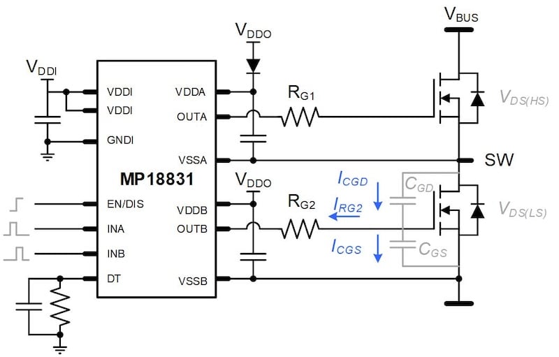
Figure 2. SiC MOSFETs in a half-bridge configuration.
Figure 3 shows this entire process. If ΔVGS(LS) exceeds the threshold voltage (VTH), then the LS-FET enters conduction as long as the gate voltage remains above the threshold, which causes shoot-through. The same is true for the opposing scenario, in which the LS-FET actively triggers and induces an undesired HS-FET turn-on.
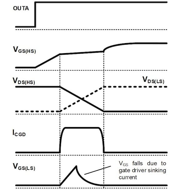
Figure 3. Current and voltage waveforms.
Now we quantify the phenomenon to determine how likely it is to occur in our design. By applying Kirchhoff’s current law (KCL) at the LS-FET’s gate node, we can calculate the Miller current (denoted as ICGD in Figure 2) as:
$$I_{CGD} = I_{CGS} + I_{RG2}$$
Equation 1.
This equation can then be expanded to:
$$C_{GD} \times \frac{dV_{DG}}{dt} = C_{GS} \times \frac{dV_{GS}}{dt} + I_{RG2}$$
Equation 2.
For high-voltage systems (VBUS >> VGS), we can approximate VDG as approximately equal to VDS. Non-idealities such as gate loop inductance, internal FET gate resistance, or the gate driver IC’s saturation current modify the gate driver’s effective sink current (IRG2). This makes it difficult to determine how the gate driver contributes to ICGD.
For simplicity, we can assume that the gate driver is unable to sink any current fast enough to prevent CGS from being charged (which occurs when IRG2 ≈ 0 A). In this case, the voltage rise on the gate is the result of a capacitive voltage divider. The change in VGS can be calculated as follows:
$$\Delta V_{GS} = \frac{C_{GD}}{C_{GS}} \times \Delta V_{DS}$$
Equation 3.
If the resulting ΔVGS does not cause the gate voltage to exceed the threshold voltage, this means that we do not need to rely on components besides the MOSFET to discharge the gate. Since CGD is not a constant value and varies with VDS, using charges is more reliable. Here is an alternative equation that indicates the odds of surpassing the threshold voltage in relation to the charge balance:
$$\frac{Q_{GD}(V_{DS})}{Q_{GS(TH)}(V_{SSO})}$$
Equation 4.
Equation 4, also known as the Miller ratio, relates two charges. The first is the charge displaced on CGD due to an increase of VDS. The second is the charge required by CGS to reach VTH (from the turn-off voltage rail, VSSO). Similarly, if the ratio is below 1, additional elements are not needed for safety. This method is often more convenient than Equation 3 because values can be easily extracted from the MOSFET’s datasheet parameters. This formula is just an approximation. Because the gate driver tries to keep the device off, it is necessary to consider how the gate driver’s charge sink impacts the ratio.
Obtaining the Miller Ratio from Datasheet Parameters
The gate charges that are indicated on the electrical characteristics chart are discrete (see Table 1). Note that these values are specific to the conditions listed below.
Table 1. Gate charge parameters in a SiC cascode datasheet.
| Parameter | Symbol | Conditions | Min | Typ | Max | Units |
| Threshold gate-to-source charge | QGS(TH) | VDS = 400V, ID = 50A,
VGS = 0V to 12V |
|
14 |
|
nC |
| Plateau gate-to-source charge | QGS(PL) |
|
26 |
|
nC | |
| Gate-to-drain charge | QGD |
|
6 |
|
nC | |
| Total gate charge | QG |
|
50 |
|
nC |
The test conditions are set to be realistic for the final application (e.g., the usual bus voltages and recommended driving rails). A quick inspection of the chart values gives us an idea of the chosen transistor’s Miller ratio. If the final application differs from the test conditions, we can check the typical gate charge curve and linearly extrapolate the values for different voltage rails (see Figures 4 and 5).
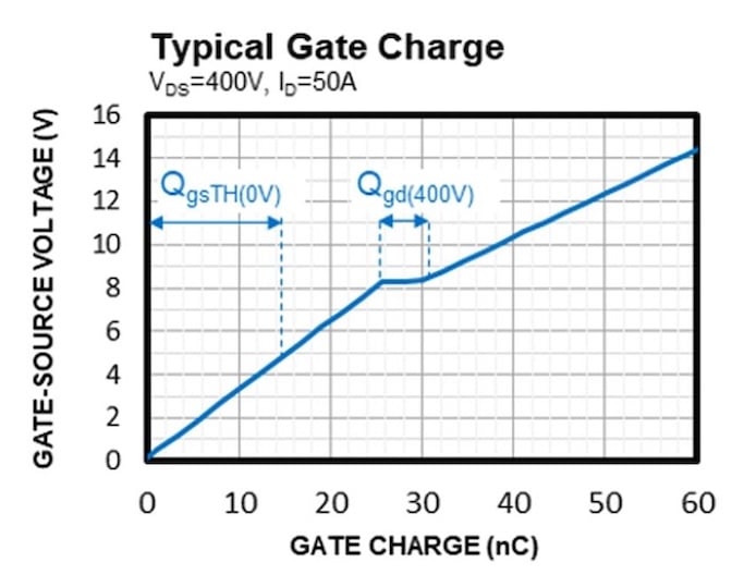
Figure 4. Gate charge curve from the datasheet.
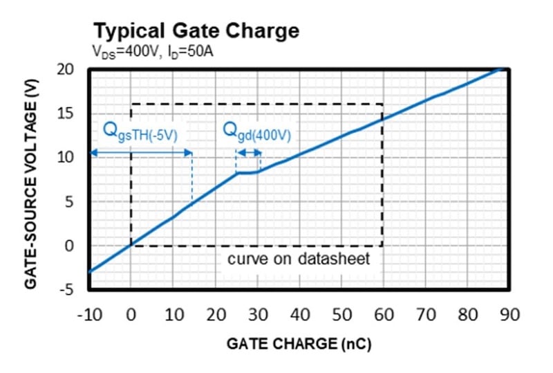
Figure 5. Gate charge curve with the extended axis values.
Mitigation Techniques
A few methods to reduce the Miller turn-on and enhance the FET from the driving perspective are described below.
Pick a Discrete Device with a Favorable Miller Ratio
Picking a FET with an optimal Miller ratio is the most obvious method to reduce the turn-on effect, as it eliminates the need for overengineering. As explained above, once a designer knows the maximum drain-to-source voltage at which the switch operates, designers should calculate the worst-case QGD/QGS for the driving conditions. If the calculated value is below 1, then the device is safe.
Increase the Gate-to-Source Capacitance (CGS)
This is a simple troubleshooting method. Any capacitor placed between the gate and the source pins of the power FET is added to the internal CGS, which improves the Miller ratio. The tradeoff is that boosting this capacitance also increases the gate driver’s power consumption, and the equivalent gate capacitance to charge/discharge each cycle also increases.
Use a Lower Ohmic Value Turn-Off Gate Resistor (RGOFF)
By using a turn-off gate resistor (RGOFF) with a low ohmic value, we can push the gate driver to sink the gate charge more quickly when the Miller current appears. This prevents CGS from being charged excessively and does not increase the gate driver’s power consumption. If you use this approach, also consider a good layout design with reduced gate-loop inductance. Otherwise, the driver circuit may not be able to evacuate the charges fast enough (see Figure 6). In addition, this solution comes with a tradeoff: Imposing a low-value RGOFF also sets a higher turn-off slope and may create other EMI issues.
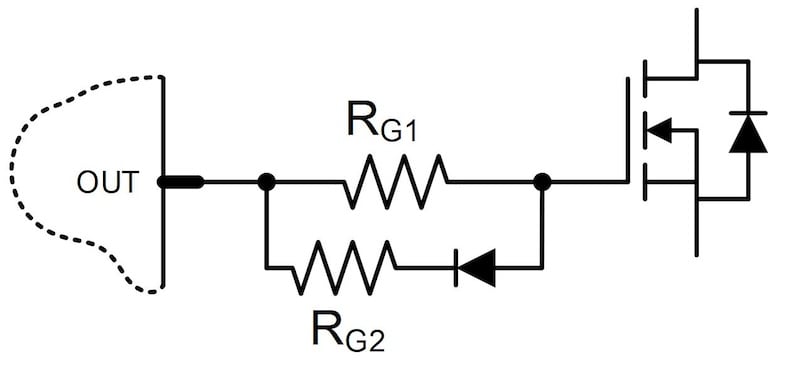
Figure 6. Typical configuration to obtain lower RGOFF than RGON on single-output gate drivers.
Use (or Increase) the Negative Rail
Setting a negative voltage at which the transistor turns off (VSSO), or increasing the negative voltage if it is already in place, is an alternative way of extending QGS(TH) (see Figures 4 and 5). The main concern for the designer is how to add a negative supply rail for the gate driver’s circuitry. When using a negative rail, a classic bootstrap technique for the high-side driver supply does not work. This may be an inconvenience for compact or low-cost designs.
Active Miller Clamp
To avoid shoot-through without jeopardizing the controllability of the gate, we can use Miller clamp circuitry. Some monolithic gate driver ICs, such as the MPQ18811, implement this feature (see Figure 7). In this figure, the clamp discharge path is highlighted in blue.
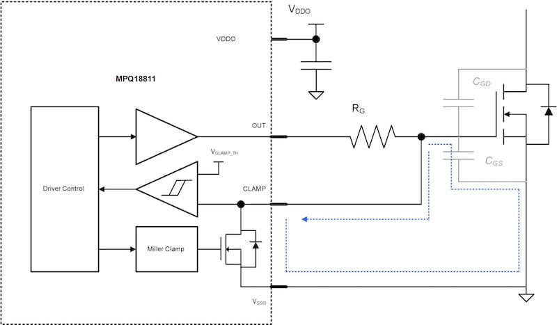
Figure 7. Active Miller clamp diagram in the MPQ18811 with clamp discharge path.
The Miller clamp operates in the following manner: shortly after the device has been turned off (VGS almost reaches VSSO) the driver activates the circuitry to clamp the gate. This creates a very low-impedance path between the gate and VSSO (see Figure 8). This path has to be minimized in the layout for optimal results. Because the clamp circuit is an alternate path for the gate loop, it can independently turn our device on and off with the preferred gate resistances and driver rails.
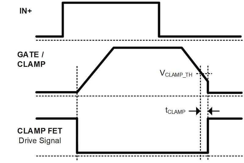
Figure 8. Operation chronogram.
Conclusion
This article explained the induced turn-on due to the Miller effect on SiC MOSFETs and SiC cascodes. This article also discussed several techniques to prevent the induced turn-on for power FETs with a high Miller ratio.
First, the Miller ratio is a good indicator when trying to determine a power FET’s immunity against this phenomenon. Second, the internal structure of silicon carbide cascodes exhibits a reduced reverse transfer capacitance, which improves robustness against the induced turn-on (in relation to its SiC MOSFET counterparts).
Lastly, gate driver ICs such as the MPQ18811 include a Miller clamp. This peripheral is specifically designed to address this issue independently of the FET’s internal parameters or gate driver conditions. A Miller clamp allows the designer to drive any type of power FET without worrying about parasitic Miller turn-on.
In addition to the MPQ18811, MPS offers other automotive-grade gate drivers to suit a variety of applications.
Related Content