 Facebook
 Google
 GitHub
 Linkedin
Resolving the Signal Part 10: How Clock Signals Affect Precision ADCs
Part 10 of the Resolving the Signal series covers how clocks affect precision ADCs, touching on clock jitter, clock intermodulation and best PCB layout practices for clocking.
Part 10 of the Resolving the Signal series covers how clocks affect precision ADCs, touching on clock jitter, clock intermodulation and best PCB layout practices for clocking.
This article was co-authored by Ryan Andrews, applications engineer for precision analog-to-digital converters at Texas Instruments.
As discussed in part 9 of this series, all data acquisition (DAQ) systems require a reference point. In that article, the reference point was a voltage level that was compared to the analog input signal to generate an output code. However, DAQ systems also require another type of reference point, though not one necessarily related to voltage.
In a DAQ system, clocks serve as the time reference such that all components can operate synchronously. For analog-to-digital converters (ADCs), accurate and stable clocks ensure that the host sends commands to the ADC and the ADC receives commands from the host in the correct order and without corruption. More importantly, the system clock signal enables the user to sample the inputs and send data whenever he requires such that the entire system operates as intended.
Although you may think of clocks as digital input signals, these components can affect the analog performance of precision DAQ systems. To further understand how clocks affect precision ADCs, we’ll discuss these topics as they relate to clock signals:
- clock jitter;
- clock intermodulation; and
- the best printed circuit board (PCB) layout practices for clocking.
Clock Jitter
While you may expect an ADC’s sampling period to be perfectly constant, there is always some deviation from the ideal. “Clock jitter” refers to the variation in a clock waveform’s edges from one period to the next. Since all ADCs use a clock edge to control the sampling point, clock-edge variation results in deviations in the sampling instance. This deviation results in a non-constant sampling frequency that appears in the conversion result as another source of noise.
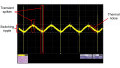
Similar to most noise sources discussed so far in this series, clock jitter is random and follows a Gaussian distribution. As a result, the sampling uncertainty error is also Gaussian, behaving just like thermal noise. Ultimately, the effect of clock jitter on ADC performance is primarily an increase in the ADC’s noise floor and, subsequently, the total thermal noise of the signal chain. Figure 1 shows the sampling-edge variation caused by clock jitter on a sinusoidal input signal.

Figure 1. Clock signal showing sampling-edge variation due to jitter
The amount by which the thermal noise increases depends on the input signal’s slew rate and the amount of clock jitter in your clock source. You can calculate the theoretical upper limit of the ADC’s signal-to-noise ratio (SNR) using Equation 1:

where fIN is the input signal frequency and tJITTER is the clock source’s jitter specification. For signals with higher frequency content, you can expect the input signal slew rate to be higher and the SNR degradation from clock jitter to be worse.
One key benefit to oversampling converters like delta-sigma ADCs is that the ideal SNR improves when using higher oversampling ratios (OSRs). Oversampling averages multiple conversions over a defined period of time, which in turn averages out some of the sampling variation caused by clock jitter. Equation 2 quantifies the SNR improvement due to oversampling, which is simply an extension of Equation 1 that adds a term dependent on the delta-sigma ADC’s OSR:

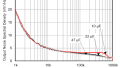
To visualize the performance difference between an ADC with oversampling and one without, Figure 2 plots Equations 1 and 2 as a function of input signal frequency and jitter. Each plot includes curves for four different clock jitter specifications (0.5 ns, 5 ns, 50 ns and 500 ns). Figure 2a represents the SNR for an oversampling ADC, while Figure 2b represents the SNR for an ADC without an oversampled architecture.

Figure 2. SNR plots for oversampling ADCs (a); and other ADCs (b)
Given the benefits of oversampling, the four plots in Figure 2a offer a 21-dB improvement in SNR compared to the equivalent jitter specification curves in Figure 2b. However, both plots illustrate the same effect: As you increase the input signal frequency or amount of clock jitter, the resulting SNR decreases. Therefore, applications with higher SNR targets may require more expensive, higher-power clocking solutions to minimize the jitter.
For example, the evaluation module (EVM) for the Texas Instruments (TI) ADS127L01, a 512-kSPS, 24-bit delta-sigma ADC, uses the Abracon ASEMB-16.000MHZ-XY-T low-jitter oscillator. This oscillator offers a typical period jitter specification of 5 ps, far lower than any of the jitter specifications plotted in Figure 2. However, if you consider the cost vs. performance trade-off for low-jitter oscillators, you might wonder if this choice is necessary or simply overkill.
To help answer this question, Table 1 compares the data-sheet noise specifications for the ADS127L01 using the “Wideband 1” digital filter setting with the SNR upper limit calculated for both 5 ps and 500 ps of clock jitter. The SNR upper-limit calculation uses the digital filter passband frequency as “fIN” to represent the maximum input signal frequency, which is where the effect of clock jitter is most apparent.
When tJITTER = 5 ps, all calculated SNR values (highlighted in green) are greater than the ADC’s data-sheet SNR specifications. Using this clock source, you could safely assume that the noise from clock jitter would not be your system’s dominant noise source. Compare that to entries highlighted in red representing the SNR values that fall below the ADC’s SNR specifications, all of which are for tJITTER = 500 ps. In this case, the noise from clock jitter would actually limit the ADC’s achievable SNR when using the full signal bandwidth.
Table 1. TI’s ADS127L01 “Wideband 1” filter SNR vs. SNRUpper Limit with 5 ps and 500 ps of clock jitter

Another key takeaway from both Table 1 and Figure 2 is that increasing the OSR (which is equivalent to slowing down the ADC’s output data rate) improves the SNR performance even further. In general, systems that can support slower output data rates are measuring slower-moving input signals. These systems will experience less noise due to jitter as the slight variations in the clock edges effectively go “unnoticed.”
Finally, one additional way that you can reduce the noise caused by clock jitter is by choosing an ADC that uses an integrated clock divider to produce the modulator sampling clock, such as the ADS131A04. A clock divider acts on only one of the two input clock edges (typically the rising edge) to produce an output clock frequency that is no more than half of the original input clock frequency. Since you can reasonably assume that some jitter exists on both input clock edges, dividing the clock in half effectively reduces the jitter on the output clock. If you continue to divide down the input clock multiple times, you further lessen the effect of the input clock’s jitter on your ADC.
Clock Intermodulation
Another way clock sources affect ADC noise performance and increase system noise is through clock intermodulation. Virtually all DAQ systems have multiple switching components that require a clock input. In some cases, these clock inputs may require different input frequencies that may be derived from separate clock sources.
If these clock sources are discrete and asynchronous, they can potentially couple with each other and produce tones in the frequency spectrum. Given two clock sources at frequencies F1 and F2, the difference or sum of their fundamental frequencies produces intermodulation tones. These are called second-order intermodulation products and are shown in Figure 3.

Figure 3. Intermodulation products due to asynchronous clock sources
Moreover, the sum or difference between the fundamental frequencies and other intermodulation products, including their harmonics, produce additional higher-order tones. While these tones may exist beyond your signal bandwidth of interest, they can still alias into the ADC passband and degrade AC specs like SNR and total harmonic distortion.
The fast Fourier transform (FFT) in Figure 4 illustrates these intermodulation effects. Using an ADC with shorted inputs (a 0-V differential input), the processor clock was set to 12 MHz while the ADC modulator clock was reduced to 11.996 MHz, creating a difference of 4 kHz.

Figure 4. FFT showing intermodulation tones at multiples of 4 kHz
Due to the difference in the processor and ADC clocks, a second-order intermodulation tone appears in the frequency spectrum at 4 kHz, with additional harmonics produced at multiples of 4 kHz. This illustrates how intermodulation products may fall directly into the passband of the ADC and contribute noise.
To mitigate this problem, wide-bandwidth applications often use one clock source to generate all other frequencies used in the system to ensure that they are all synchronous. Another useful mitigation technique is to choose clock frequencies and sampling rates that are least likely to produce tones within the signal bandwidth of interest.
Best PCB Layout Practices for Clocking
When designing the PCB layout for your clock source, take care to keep the clock signal as clean as possible. Although it is considered a digital input, treat the clock signal as if it were another important analog signal. Minimize trace impedances, route traces away from Serial Peripheral Interface (SPI) signals and other noisy circuitry, and consider including PCB footprints for a series resistor and shunt capacitor to help handle reflections or overshoot. Figure 5 shows an example clock layout from the ADS127L01EVM.

Figure 5. Example clock layout
The red line in Figure 5 traces the clock path from the source to the ADC (U26, highlighted in red). The clock path begins with the clock source (Y1), which is then fed into a clock fan-out buffer (U23). Both of these components are highlighted in blue in the top right corner of Figure 5. The clock fan-out buffer generates two identical copies of the original input clock frequency: one to drive the ADC and another to drive a microcontroller (through R55).
To go to the ADC, the clock signal continues on through a small 43-Ω resistor (R56) in series with the clock buffer output to help dampen reflections. The clock signal then connects to a jumper (JP6) that selects one of three different ADC clock frequencies. The other two clock frequencies are produced by two D flip-flops (U24 and U25, highlighted in yellow in Figure 5). These components divide down the clock buffer output to produce the clock for the other two modes: “low power” (LP) mode and “very low power” (VLP) mode. All three mode choices are also synchronous to the original clock source. In Figure 5, the solid red line passes through the “high resolution” (HR) mode selection.
After the jumper, the selected clock signal passes through another resistor (R60) and a shunt capacitor (C76) before reaching the ADC clock pin. The path is kept as short and as direct as possible. The SPI interface signals (highlighted in green) are also kept away from the clock input until they reach the ADC.
Additional Clocking Tips for Best Performance
If you follow the clock layout guidelines provided here but still suspect that your clock is degrading your ADC performance, there are some additional clock-related issues to test.
The Clock Signal Quality at the ADC Input
If the clock signal at the ADC clock input pin shows excessive overshoot and ringing, you may need to slew the clock edges further by adding or increasing the size of the small series resistor and shunt capacitor (R60 and C76 in Figure 5, respectively). Adding these components effectively applies a low-pass filter to the clock input while preserving the fundamental clock frequency.
You may also notice what appear to be “shelves” or “steps” in the clock edges. This is caused by reflections of the clock signal as it travels along a trace and runs into a high-impedance input. A series resistor will help dampen these clock reflections.
The Supply Pins on the ADC
Because both the ADC’s DVDD input and the clock source or clock buffer may share the same digital supply, check these pins for large transients. Transients result from sudden demands in current and may require additional decoupling capacitors to suppress. But take care when choosing the size of your decoupling capacitors: smaller decoupling capacitors have less inductance and can supply the necessary current more quickly, while larger decoupling capacitors help store the bulk of the necessary charge and filter any noise on the supply rail. A combination of both decoupling capacitor sizes may be necessary to keep the digital supplies quiet and stable.
Another technique to help reduce transients from coupling into the ADC output is to place a small ferrite bead between the ADC digital supply pin and the clock source or clock buffer supply pins.
Split the Ground Plane
If your PCB’s size prohibits placing clock circuitry far away from sensitive analog circuitry, it may help to partially split the ground in order to isolate the clock current’s return path. However, always tie back both sides of your ground plane as close to the device as possible to avoid significant ground potential differences between the ADC’s analog and digital sections.
Ridding Signal Chains of Clock Source Noise
Ultimately, following the practices and procedures recommended in this article should help to avoid the most common clocking-related issues and ensure that your clock source is not the biggest contributor of noise to your signal chain.
In part 11 of the “Resolving the Signal” series. we’ll discuss the impact of power supplies on precision ADCs.
Related Content


tutorial needs to some equipments
Thanks for the great tutorial series. Looking forward to the next installment.