Facebook
 Google
 GitHub
 Linkedin
Resolving the Signal Part 9: Reducing Reference Noise in High-Resolution Delta-Sigma ADC Circuits
Part 9 of the Resolving the Signal series analyzes several different methods for reducing reference noise's effect in systems and examines the difference of reference noise's impact on low- and high-resolution ADCs.
Part 9 of the Resolving the Signal series analyzes several different methods for reducing reference noise's effect in systems and examines the difference of reference noise's impact on low- and high-resolution ADCs.
In part 8 of the Resolving the Signal series, I discussed the relationship between analog-to-digital converter (ADC) noise and reference noise, derived an equation for calculating reference noise, and determined the effect gain has on the level of reference noise in a system.
In part 9, I’ll conclude the discussion of reference noise by analyzing several different methods for reducing its effect on the overall system. I’ll also examine the difference between the impact of reference noise on low- and high-resolution ADCs.
Reducing the Effect of Reference Noise
As I discussed in part 8, the amount of reference noise that enters a data acquisition system depends on the reference source’s noise performance as well as the percent utilization of the full-scale range (FSR). To demonstrate this reliance on percent utilization, I plotted ADC noise, reference noise and total noise as a function of the full-scale utilization (input voltage) assuming a 2.5V reference. Figure 1 shows a plot of this relationship using the Texas Instruments (TI) ADS1261, a 24-bit delta-sigma ADC with an integrated programmable gain amplifier (PGA).
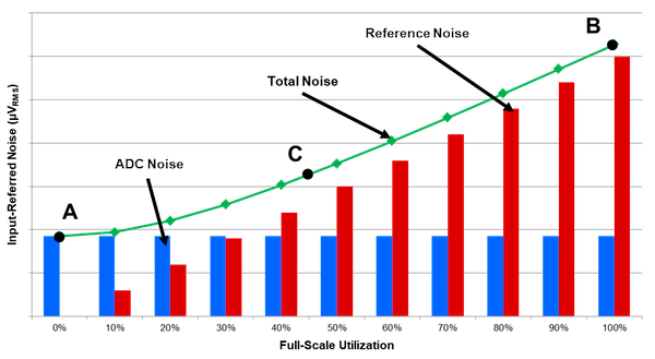
Figure 1. ADC noise, reference noise, and effective resolution as a function of FSR utilization
As in part 8, reference noise begins to dominate the system’s total noise at a utilization factor of 40%, nullifying the noise benefit provided by a high-resolution ADC. To help mitigate this issue and achieve precision systems, there are three techniques to help decrease reference noise and take advantage of the noise-reduction benefits of delta-sigma ADCs.
Choose a Lower-Noise Reference
One of the most obvious ways to reduce the level of reference noise entering a system is to choose a voltage reference with less noise. This has the effect of reducing the level of the red bars in Figure 1 and extending the useful FSR utilization limit.
However, as I suggested in part 8, take care to match the level of reference noise to the level of ADC noise for any given input signal. For example, if you sample a 2.5V input signal using the ADS1261, you could only use a gain of 1V/V. In those circumstances, choosing a voltage reference with less noise than the REF6025 will likely have little effect on overall system noise, since the FSR utilization is so high (Figure 1).
Increase the Reference Voltage
Another method to potentially reduce the effects of reference noise is to increase the reference voltage, as this affects a change in the percent utilization. For example, doubling the reference voltage decreases the percent utilization by a factor of 2. However, this method only offers a system noise benefit if there is no proportional increase in reference noise, which is not always the case. Many discrete voltage reference families specify noise in microvolts per volt because the reference noise scales linearly with the reference voltage. In this case, doubling the reference voltage also doubles the reference noise, yielding no system noise benefit despite a decrease in percent utilization.
Reduce the Effective Noise Bandwidth
A third option to reduce the amount of reference noise passed into the system is to limit the overall effective noise bandwidth (ENBW). One way you can limit the ENBW is by reducing the anti-aliasing or reference filter cutoff frequencies. However, Texas Instruments recommends using C0G-type capacitors for input signal-path filters due to the C0G’s low voltage and temperature coefficients. Typical C0G capacitors used in signal-chain design are only available up to 10-15nF, inherently limiting how low the anti-aliasing filter cutoff can be. Conversely, reference filters may employ higher-capacitance, X7R-type capacitors due to the voltage reference’s virtually constant DC output voltage. For each filter type, use low-drift, low-impedance resistors (<10kΩ), because the resistor’s thermal noise increases with impedance and may begin to dominate the signal-chain noise.
A more common method to reduce the system ENBW is to slow down the ADC’s output data rate. Figure 2 shows how reducing the ADC’s output data rate decreases both the ADC and reference noise simultaneously. For example, between ENBW = 96Hz (left) and ENBW = 0.6Hz (right), the reference noise at 100% utilization has decreased by a factor of 2.3, while the ADC noise has decreased by a factor of 10, resulting in far less total noise.
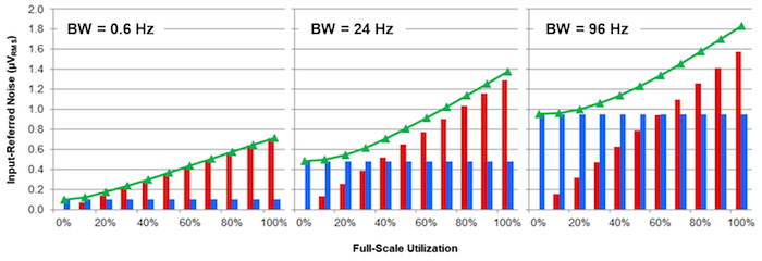
Figure 2. Limiting ENBW reduces total noise: 0.6Hz (left), 24Hz (middle), 96Hz (right)
While these three methods can mitigate reference noise for many applications, other systems may have fixed parameters – such as settling time or sensor-output voltage – that make these techniques harder to employ. In such instances, you can reduce the amount of reference noise passing into the system by choosing an appropriate reference configuration: internal, external or ratiometric.
Internal References
Precision ADCs often include integrated precision voltage references that are generally suitable for many applications. An integrated reference eliminates the added cost, area and power consumed by an external reference. However, in general, internal references are lower power and may have higher noise and higher drift compared to precision external references, making them less suitable for some high-precision and high-accuracy systems.
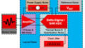
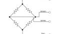
Figure 3 shows the ADS1261 measuring a resistive bridge while using its integrated voltage reference as the reference source for the measurement.
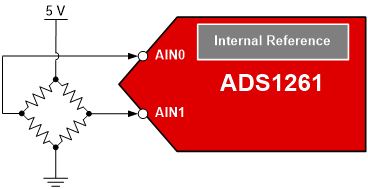
Figure 3. Measuring a resistive bridge using the ADS1261’s internal reference
External References
If the specifications of an integrated voltage reference are insufficient and the ADC allows for an external reference source, you can choose an external reference instead. External references generally benefit from lower noise and better drift parameters relative to integrated references. This increased performance comes at the expense of higher power consumption, additional cost and increased printed circuit board (PCB) area. Also, since the ADC and voltage reference do not share the same die, their temperature drift specifications may no longer be correlated; this is the case with an integrated reference. Therefore, the ADC and reference can drift independently and in opposite directions, causing greater inaccuracy. To avoid this issue, connect both devices to a good, thermally conductive ground plane.
A helpful hint when connecting an ADC to an external reference source is to route the ADC’s negative external reference input (REFN) back to the ground pin of the external reference instead of connecting REFN directly to the PCB’s ground plane. This makes a “star” ground connection that helps avoid ground plane noise pickup on the negative reference input and maintain precision measurement results.
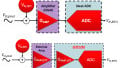
Figure 4 shows the same resistive bridge connection diagram as in Figure 3, but using a REF6025 voltage reference instead of the ADS1261’s internal reference.
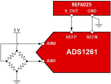
Figure 4. Measuring a resistive bridge using the ADS1261 and an external reference (REF6025)
Ratiometric References
Where sensor excitation is necessary, such as measuring resistive bridges or resistance temperature detectors (RTDs), use a ratiometric configuration. This configuration uses the same excitation source for the analog input and reference voltage. As a result, any noise or drift in the excitation source will affect the measurement and the reference equally. Since the ADC output code is a ratio of the input to the reference, the excitation source noise and drift tend to cancel, resulting in noise performance that is much closer to the shorted-input case. In general, this configuration yields the lowest amount of total noise compared to the other two configurations.
The main disadvantage of the ratiometric reference is that it can only be used for applications where sensor excitation is necessary. As a result, if the system doesn’t require sensor excitation, you must choose one of the other two reference configuration options.
Figure 5 shows the same circuit as in Figures 3 and 4, but with a ratiometric reference configuration. Note how the 5V bridge excitation voltage is also used as the ADS1261’s external differential reference voltage (REFP - REFN).
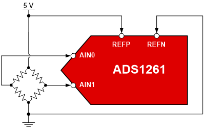
Figure 5. Measuring a resistive bridge using the ADS1261 and a ratiometric reference
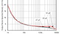
So far, I’ve made the qualitative claim that a ratiometric reference provides better noise performance than an external reference, which provides better noise performance than an internal reference. If you look at the data sheet for TI’s 24-bit ADS1259, you can see that this is quantitatively true as well. Figure 6 shows a plot from the ADS1259’s data sheet that includes measured noise performance for all three configurations.
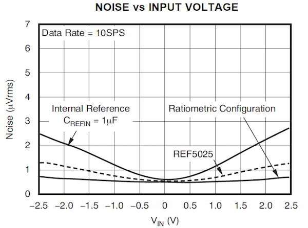
Figure 6. Comparing the total noise increase from internal, external and ratiometric reference configurations with the ADS1259
At VIN = 0V, the plot in Figure 6 shows the ADS1259’s inherent noise to be approximately 0.5µVRMS. At 100% utilization (VIN = ±2.5V), the internal reference increases this baseline noise by 400% to 2.5µVRMS, while the external REF5025 increases the total noise by 150% to 1.25µVRMS. Compare those curves to the almost-flat ratiometric reference curve, which increases the total noise by only 50% at 100% utilization. This configuration allows you to use the entire FSR of the ADS1259 without increasing total noise by a significant amount, resulting in the best overall system noise performance.
Can you apply these conclusions equally to all delta-sigma ADCs? So far in this series, I have analyzed 24- and 32-bit converters to get a better understanding of how voltage reference noise affects the performance of these devices. In general, these high-resolution ADCs offer very low noise such that any reference noise has a noticeable effect on system noise. How does reference noise impact lower-resolution ADCs?
Lower- Vs. Higher-Resolution ADCs
You can apply the same principles used to measure reference noise’s impact on higher-resolution ADCs to lower-resolution ADCs. Using the same setup from the previous examples, let’s connect the REF6025 to ADCs with different resolutions and measure the total noise at 100% utilization. Figure 7 depicts this setup.
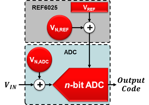
Figure 7. System setup using the ADS1262 and REF6025
Let’s choose eight ADCs with different resolutions to act as the n-bit ADC in Figure 7. Table 1 provides baseline noise information for each ADC as a function of its resolution.
Table 1. Inherent ADC Noise by ADC Resolution
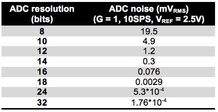
As I discussed in part 1 of the series, quantization noise usually dominates a lower-resolution ADC’s total noise (<16 bit) such that its value corresponds to the least significant bit (LSB) size. On the contrary, 18-, 24- and 32-bit ADC noise is larger than the corresponding LSB size due to the relatively larger amount of thermal noise in higher-resolution ADCs.
To calculate the combined noise of the ADC and voltage reference, take the root-sum-of-squares (RSS) of the noise of each component since I assumed 100% utilization. Table 2 includes the resulting total noise of both components, as well as the percentage increase in noise compared to just the ADC’s noise.
Table 2. Total Noise and Percentage Increase by ADC Resolution
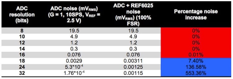
Table 2 offers a stark contrast between the effects that reference noise has on lower- and higher-resolution ADCs. Up to approximately the 16-bit level (the red highlighted cells in Table 2), the REF6025’s noise has virtually no impact on the total noise of the system, even at 100% utilization. In these cases, the high levels of ADC quantization noise outweigh the lower levels of reference noise. Therefore, the low-noise external reference provides little benefit here, especially when compared against the increased system cost and size. In fact, many lower-resolution ADCs do not include external reference inputs for this reason, and instead relies on an integrated reference or even the supply voltage to perform this function.
However, this does not imply that you should never be concerned with reference noise when using lower-resolution ADCs. The cumulative effect depends on the noise of the specific voltage reference, the system bandwidth and the percent utilization. I recommend performing some quick calculations to determine the general effect any external components might have on the system.
Where reference noise always has a greater impact is on the 18-, 24- and 32-bit higher-resolution ADCs (the blue highlighted cells in Table 2). All of these ADCs experience a significant increase in noise relative to the ADC by itself. This result is more pronounced as the ADC resolution increases, with the 32-bit ADC experiencing an incredible 553% increase in noise due to reference noise alone. At the higher-resolution levels, using the noise-reduction methods outlined in this article and choosing an appropriate reference configuration are critical to maintaining precision measurements.
In part 10 of Resolving the Signal, I'll discuss how clocks affect precision ADCs.
Key Takeaways
Here is a summary of important points to help better understand how voltage reference noise affects delta-sigma ADCs:
- Reducing reference noise:
- Use a low-noise reference
- Reduce your ENBW
- Increase the reference voltage (as long as the reference noise does not increase proportionally)
- Use a ratiometric configuration
- Optimize system noise performance by choosing a reference configuration that provides reference noise performance similar to your ADC’s noise performance.
Related Content