Facebook
 Google
 GitHub
 Linkedin
Shorten Hardware Development Cycles by Parallelizing Firmware and PCB Design
Learn to decouple application logic from physical routing using a Board Support Package (BSP). This layered architecture accelerates prototyping and minimizes costly respins on custom boards.
Software teams ship and iterate daily. Hardware teams traditionally serialize processes: design the board, wait weeks for fabrication, then start firmware and discover problems that force an expensive respin. This article shows how to collapse that loop by developing firmware in parallel with PCB layout, using an STM32 Nucleo board and STM32CubeIDE.
The article goes into concrete implementation. It shows how to structure firmware so the same codebase targets both the dev kit and a future custom board, separating board support (clock, pin assignment, peripheral instances) from application logic so migration is just a configuration change, not a rewrite. It walks through a worked example, bringing up a representative peripheral on the Nucleo via CubeMX, then identifying exactly what must change when moving to custom boards.
Finally, it also covers what a dev kit cannot tell you, such as analog front end (AFE) behavior, power integrity, and real-world signal conditions. The goal is a concrete, reproducible workflow that lets small hardware teams iterate much closer to software velocity.
The Strategy: Decoupling Application Logic from Hardware
Many firmware changes that occur during custom board development are driven by tight coupling. You need to avoid writing application logic that writes to specific registers or calls highly dependent Hardware Abstraction Layer (HAL) functions for specific pins because that will constrain your code to a tight hardware layout.
Instead, implement a layered architecture with the following layers:
- Application Layer: not dependent on the physical pins or peripheral instances you are using; uses business logic like processing sensor data or handling state machine transitions.
- Hardware Abstraction Layer (HAL/BSP): Ties more abstract application requests to physical pin assignments, registers, and clock configurations.
When you are transitioning from an off-the-shelf board like the STM32 Nucleo board to your highly customized miniature board, you only need to modify the configuration (BSP) layer and should not modify the core application logic. Figure 1 illustrates the layered architecture flow for switching from a Nucleo board to a custom PCB.
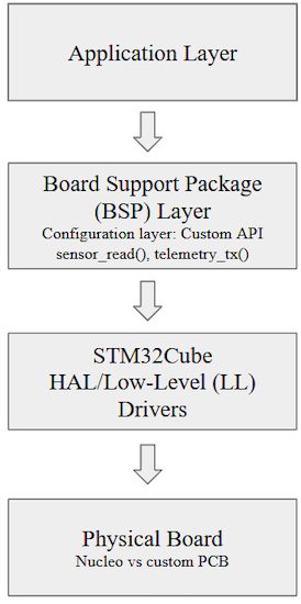
Figure 1. Layered architecture flow for switching from Nucleo board to custom PCB.
Code Architectures: What NOT to Do vs. What to Do
To appreciate this simplified layered architecture approach, let’s look at an example of a peripheral bring-up where the goal is to read a 3-axis digital accelerometer over an I²C bus. In the code below, the register addresses used (WHO_AM_I at 0x0F, output registers starting at 0x28, and device address at 0x19) are taken from the ST LIS3DH/LIS3DSH family layout. You can replace them with your own part’s datasheet values. There are two versions of this code: What NOT to Do and What To Do.
What NOT to Do: Tightly Coupled Code
What to Do: Abstraction via Board Support Package (BSP)
Instead, write two files to integrate hardware changes: bsp_sensor.h and bsp_sensor.c. These are demonstrated in the following two code blocks.
The bsp_sensor.h and bsp_sensor.c files will be called in the main.c primary application layer shown here:
Setting Up the Parallel Pipeline in STM32CubeMX
When you transition away from the development kit to your custom board, all changes are made within the BSP source file and using the graphical configuration tool. As demonstrated in Figure 2, assign logical User Labels (ACCEL_SCL and ACCEL_SDA) to physical I2C pins within the STM32CubeMX Pinout view to decouple hardware layout dependencies from generation files.
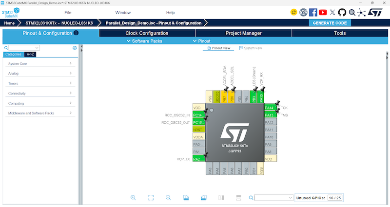
Figure 2. Assigning logical user labels to physical I2C pins within the STM32CubeMX pinout view.
First, configure the Nucleo baseline by initializing the project and selecting the Nucleo board. This will configure your main system clocks via the internal HSI oscillator and map your debug communications interface. Then assign user labels to your pins. Do this by right-clicking on your configured pins in the CubeMX pinout view. You then have the option to label the pins, for example: ACCEL_SCL, ACCEL_SDA. CubeMX will create object macros for the labels in the main.h file.
When you receive your custom PCB, you only need to make two adjustments: Open CubeMX, map I2C1 to the pins you are using, and regenerate. If using another peripheral instance, like switching to hi2c2, just change the single external reference in the bsp_sensor.c code.
Blind Spots: What a Dev Kit Cannot Tell You
Although this parallel pipeline reduces delays in code bring-up, it is important to know that it is much easier to work with a development kit. Also, what might work on a workbench with a dev kit does not necessarily work on an intricate PCB. Here are a few blind spots to watch out for while designing your board.
Power Integrity and Transient Resets
The Nucleo board has bulk capacitance and a stable power supply from the ST-LINK USB debugger. Your PCB will most likely have a compact switching regulator or lithium battery. If you place your switching inductor right next to the MCU’s analog supply pin (V_DDA) or if you elect to use few low-ESR ceramic decoupling capacitors (0.1 µF paired with 4.7 µF bulk capacitance), you might face unpredictable resets on your firmware whenever high-current subsystems activate.
Analog Front End (AFE) Signal Integrity
Dev kits don’t shield noise very well. This means that if you are prototyping on a Nucleo breadboard, for example, and are using long jumper wires to read microvolt signals from an analog sensor, you will run into large electromagnetic interference. This is why it’s important to design the layout efficiently ahead of time.
When designing the layout, keep a single unbroken ground plane and control noise by designing better placement and routing. This includes grouping analog components together and separating noisy digital and switching traces from analog traces and their return paths.
Figure 3 demonstrates a complete physical interface mapping. An I2C sensor module is connected to the STM32 Nucleo-L031K6 board using these primary hardware lines:
- I2C1_SCL (PB6 / D1)
- I2C_SDA (PB7 / D0)
- External hardware interrupt line PA0 (A0)
- Address grounding (AD0)
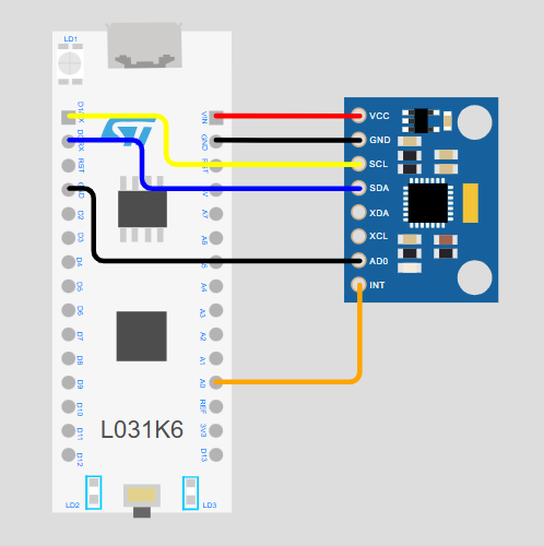
Figure 3. Complete physical interface mapping.
Bridging the Handoff: The Shared Verification Protocol
Parallel development is only efficient if both the hardware and firmware engineers are on the same page. During layout development, use the table below as a checklist for both teams.
Table 1. Layout development checklist
| Verification Stage | Action Item | Hardware Diagnostic Tool | Firmware Validation State |
|---|---|---|---|
| Phase 1: Bare Metal Safety | Validate that power rails match specifications. Check for shorts before powering the chip. | Digital Multimeter (DMM) / Lab Power Supply with current limit set to <50 mA. | No code executed; MCU held in reset state via hardware pin. |
| Phase 2: Clock & Debug Trace | Verify internal/external oscillators lock successfully. Establish SWD communications interface. | Oscilloscope with high-impedance active probe on OSC pins. | Execute micro-kernel initialization; assert clock output configuration via MCO pin. |
| Phase 3: Bus Protocol Validation | Audit bus signaling states. Check for structural layout reflections or improper rise-times. | 4-Channel Mixed Signal Oscilloscope or Logic Analyzer. | Run isolated peripheral BSP tests (e.g., reading WHO_AM_I register). |
Following this checklist and the steps outlined in this article ensures that hardware and firmware teams are aligned. It can also help avoid long sequential iteration cycles and speed up the development process greatly for startups.
All images provided by the author.
Related Content