Facebook
 Google
 GitHub
 Linkedin
3D Printing Electronic Components? Nano Dimension Releases DragonFly LDM Manufacturing Platform
DragonFly LDM extends the scope of 3D printing to the unattended, low-volume manufacturing of electronic circuitry.
DragonFly LDM extends the scope of 3D printing to the unattended, low-volume manufacturing of electronic circuitry.
While the history of 3D printing begins back in the 1980s, widely-available 3D printers are still something of a novelty. Nowadays, a small, maker-oriented 3D printer may only cost $250, but there are much larger and complex 3D printers specifically designed to allow on-site fabrication of PCBs and even individual components.
This week, Nano Dimension introduced a new 3D printing technology, DragonFly LDM, to serve this purpose.
Nano Dimension describes this additive manufacturing process as a lights-out digital manufacturing (LDM) printing technology. This name comes from the fact that the printing requires no hour-by-hour human assistance—at all. So, the lights can, literally, be turned off on your way out the door.

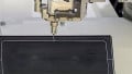
The DragonFly LDM. Image from Nano Dimension
DragonFly LDM builds on the company’s extant DragonFly Pro system. This iteration has improvements over the older version in that the print heads are automatically self-cleaned every few hours, controlled by software management algorithms. Because of this and other advancements, Nano Dimension says that only one scheduled maintenance downtime per week is needed.
3D Printing Electronics with Multi-Material Additive Manufacturing
3D printing is called additive manufacturing because three-dimensional objects are built by the sequential “adding” of material, layer by layer. What’s different about DragonFly LDM is that it supports two printheads, one can be deployed for nano-silver conductive ink and the other for dielectric polymer ink. This allows the system to concurrently print with both advanced inks in a single print job.

Rendering of Nano Dimension's multi-material additive manufacturing. Image from Nano Dimension
As illustrated in the above diagram, PCB features, such as vias and through-holes, can be fully 3D printed by the system. Subsequent etching, drilling, and plating stages are unnecessary.
The Growing List of 3D Printing Applications
Over the years, 3D printing has been introduced into applications from drones equipped with 3D-printed embedded electronics to full-sized aircraft manufacturing to research on 3D-printed wearable sensors.
In DragonFly LDM's case, the initial deployment of the system was with Hensoldt, a German innovator in the area of defense and security electronics. As described by Andreas Salomon, 3D project leader for printed electronics at Hensoldt, ”The DragonFly LDM is a necessary evolutionary setup up from the DragonFly Pro, enabling low-volume manufacturing of electronic circuits fast and easy to do in-house, with minimal operator time."
Printing Components On-Site
Modern surface-mount components are increasingly tiny. One of the reasons it's possible for the DragonFly LDM platform to fabricate them is that it has a mechanical accuracy of one micron.

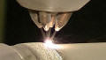
Example components and PCBs fabricated by the DragonFly LDM system. Altered images from Nano Dimension
Nano Dimension asserts that DragonFly LDM makes it possible to manufacture myriad components:
- Antennas and RFID tags
- Sensors
- Electromagnets
- Molded Interconnect Devices (MIDs)
- Multi-layer PCBs
- Capacitors
- Transmission lines up to 20 Ghz
- Transformers
Nano Dimension has various case studies and use cases available for download on their website if you'd like to learn more.
FAST Prototyping, Improved Time to Market
In addition to building electronic devices, the DragonFly LDM can also prototype them. This is a key advantage in the fast-moving arena of product design. In this manner, working devices are available in hours, rather than weeks. With this strategic capability, any design flaws are exposed almost immediately and quickly corrected. This enables a vast improvement in overall time to market.
Key features for prototyping include:
- Supports 3D-printed multilayer printed circuit boards (PCBs)
- Can build PCBs as large as 16 cm X 16 cm x 0.3 cm
- Can print layers up to 3 mm thick
- Silver nanoparticle structures are solderable
- Compatible with external files, including Gerber and ODB++
Important Specifications
- Deposition technology: Piezo drop-on-demand inkjet
- Number of printheads: Two, one for each ink
- Minimum trace layer thickness: 17 microns
- Minimum dielectric layer thickness: 35 microns
- Inks: Nano Dimension Optimized Silver nano particles and dielectric inks
- Trace conductivity relative to Copper: 5% to 30%, process-dependent
- Dielectric constant: From 2.9 @ 200MHz to 2.69 at 2GHz
- Build volume: 160mm x 160mm x 3mm
- Operating system: Windows
- Network connectivity: Ethernet TCP/IP 10/100/1000
- Regulatory compliance: UL, CE, FCC
To some, it may still seem a bit like science fiction to have a functional PCB assembly system in-house. 3D-printing components is another level of precision, however, which Nano Dimension hopes to deliver.
What are your opinions on 3D-printed components? Have you ever worked with them before? Share your experiences in the comments below.
Read More about 3D Printing
- 3D Printing Filaments Moving Beyond Plastics
- Working with High-Temperature 3D Printer Filaments
- HT vs PLA Filament for High-Temperature 3D Printing
- Teardown Tuesday: 3D-Printing Pen
- 3D Printing and Printable Electronics Combine to Change the Way We Manufacture Electronics