Facebook
 Google
 GitHub
 Linkedin
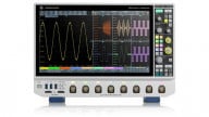
AMD Claims Planet’s Largest FPGA-based SoC for Emulation and Prototyping
The company positions the new chiplet-based SoC as well suited for todays’ ever more complex chip designs.
It’s no secret that chips are becoming increasingly more complex as fields like artificial intelligence (AI), machine learning (ML), and high-performance computing (HPC) push the state of the industry. Because of this increase in complexity, chip design—and especially test and verification—has become an enormously difficult task.

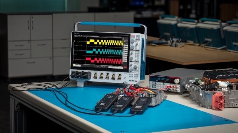
The chiplet-based Versal VP9102 SoC is comprised of four individual dies, which AMD calls super logic regions (SLRs).
Feeding those needs, today, AMD is looking to ease the pain of chip test and verification with the release of its Versal VP9102 SoC. All About Circuits had the opportunity to talk with Rob Bauer, senior product line manager for Versal at AMD to hear more about the new SoC ahead of the launch.
The Need for Emulation SoCs
One of the most important aspects of chip development is the emulation and prototyping phase of a design. Since advanced chips are so expensive to physically manufacture, designers need to have a way to actually verify their design’s functionality (outside of simulations) before committing to a tape out. To do this, designers will emulate their design on a large emulation platform (like an FPGA-based SoC), to validate the chip before entering physical production.
All that said, as modern chips become more complex, the requirements for the underlying emulation platforms become increasingly complex and costly as well. As Bauer explains “If you look at a two-nanometer advanced design, current cost estimates predict over $700 million per design—and over half of that is just in verification and software development alone.”
Two Trends Driving the Need
Two trends are largely driving this increase in complexity. The first is a general increase in gate count to keep up with compute-intensive applications like machine learning. The second is the emergence of chiplets—where designs consist of multiple dies tied together via advanced packaging technology.
As these trends drive complexity in chip design, emulation platforms will rise in importance as well. “The semiconductor devices five years from now are going to be exponentially more complex than what we have today,” says Bauer. “That means the emulation platforms are going to be even more critical than they are today.”
VP1902: A Look at Its Architecture
AMD’s Versal VP1902 SoC is described as an emulation class adaptive SoC which is designed specifically to streamline and future-proof the emulation and prototyping phase of advanced chips. AMD is claiming that the VP1902 is the world’s largest adaptive SoC based on gate size, offering 18.5M logic cells total—a number which they claim is 2x greater than the prior generation VU19P.
Speaking to the importance of capacity in emulation and prototyping, Bauer tells us that it’s all about staying ahead of the technology..
“The devices that need to be emulated keep getting bigger. So we need a bigger device to run them on, otherwise, it becomes an untenable problem to emulate those designs.“

A system block diagram of the VP1902. (Click on image to enlarge)
Underlying this enormous amount of logic is what AMD calls a “quadrant-based architecture”. The chip itself consists of four individual dies, referred to as “super logic regions” (SLRs), each interconnected by a network-on-chip (NoC).
Within each of these SLRs exists a programmable logic, a dual-core Arm A72 processing subsystem, a memory controller, SerDes blocks for high-speed connectivity with outside hardware, and a parallel digital communication interface (XPIO) to communicate with other VP1902s.
The VP1902 in Action
The cumulative result of these architectural decisions is that the VP1902 offers some impressive performance specifications.

Compared to its predecessor, the VP1902 offers significant improvements in capacity and speed.
“Historically, these emulation prototyping platforms, they're going to run the design at a lower rate than the eventual silicon especially when you talk about the fact that this billion gate or half a billion gate design might be spread over many different devices,” says Bauer. “But things like the improved I/O bandwidth and the capacity mean that we can run designs at a higher clock rate on VP1902 and get closer to that actual tape out speed.”
Future-proofing in the Face of Complexity
There’s no doubt that the chip design process is growing increasingly complex. If we are to stay on pace with the demands of the industry, improved technology in the space of prototyping and emulation is absolutely necessary.
With the VP1902, AMD is looking to provide a future-proof solution that offers more capacity and greater speeds than ever before. Hopefully, the result will be a future in which advanced chip design can be more affordable and more attainable.
AMD says that the Versal Premium VP1902 adaptive SoC is expected to begin sampling in Q3 to early access customers. Production is planned for the first half of 2024.
All images used courtesy of AMD
Related Content