Facebook
 Google
 GitHub
 Linkedin
AMD Intros Mid-Range FPGAs Targeting Intelligent, High-Performance Designs
Announced today, the new FPGAs build off of AMD’s existing ecosystem with modernized memory, I/O, and security.
Today, AMD announced a new family of mid-range FPGAs meant specifically for “intelligent, high-performance designs”. With the new Kintex UltraScale+ Gen 2 family, AMD is looking to expand on its existing FPGA offerings with modernized memory, I/O, and security subsystems while retaining continuity with its FPGA toolchain and Kintex architecture. All About Circuits spoke with AMD’s Ahmed Khalid, Senior Manager, Product Line Management, and Bryan Fletcher, Senior Product Marketing Manager, to learn about the release firsthand.
Architectural Focus on End-to-End Data Movement
The new Kintex UltraScale+ Gen 2 family is based on the premise that system performance depends on how efficiently data moves from ingestion through processing and back out of the device. As Fletcher explains, “We have increased our data handling capacity from end to end from when the data comes in until it’s stored, computed, and goes back out with results. That’s what’s required if you want to increase system performance. You’ve got to increase the amount and quality of data.”
To this end, AMD designed the device architecture to include high-speed serial transceivers, dense parallel I/O, hard memory controllers, and high compute density in a balanced pipeline.
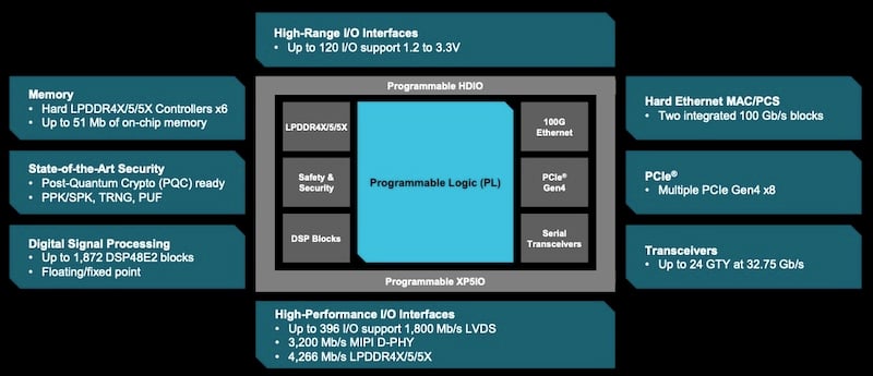
Data handling in Kintex UltraScale+ Gen 2
Specifically, the devices incorporate up to 24 GTY transceivers running at 32.75 Gb/s per lane. This transceiver density supports 100 Gb Ethernet, PCIe Gen4, and high-bandwidth video interfaces without fragmenting bandwidth across multiple devices. Two integrated 100 Gb Ethernet MAC and PCS blocks reduce logic utilization and power draw compared to soft implementations, while multiple PCIe Gen4 x8 interfaces support host connectivity with up to 128 Gb/s per interface.
Explaining the virtues of this approach, Fletcher tells us, “We’ve increased the speed and quantity of I/O, which allows for additional sensors with the analog front end running at higher frequencies. The memory bandwidth is significantly increased while the processing capacity has also been boosted because of embedded efficient hard blocks.”
AMD also focused its attention on parallel I/O offerings. The XP5 I/O subsystem supports up to 396 high-performance pins per package, with each interface operating at 1.8 Gb/s for LVDS and 3.2 Gb/s for MIPI D-PHY. The same I/O fabric supports LPDDR4X, LPDDR5, and LPDDR5X memory signaling at data rates up to 4.266 Gb/s.
Gains Over Prior Generations
AMD reports up to a five-times increase in aggregate external memory bandwidth compared to previous Kintex UltraScale+ devices. The company attributes these gains to the inclusion of up to six hard 32-bit LPDDR memory controllers per device, whereas earlier generations relied on soft DDR controllers with narrower effective bandwidth and higher logic overhead.
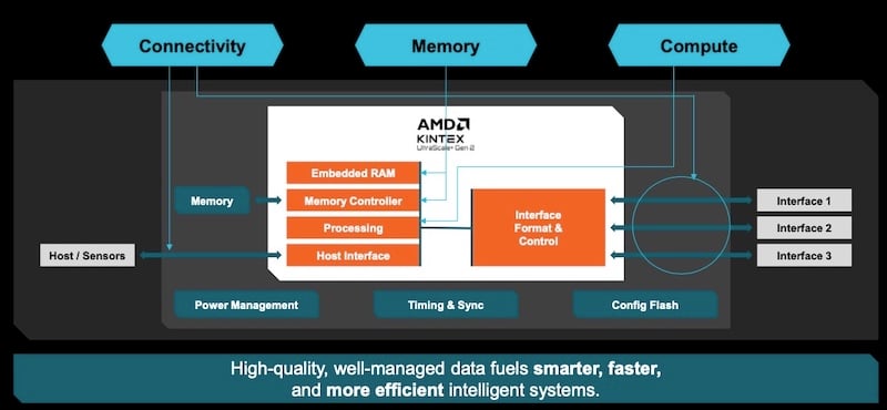
An example application block diagram based on the Kintex UltraScale+ Gen 2
Meanwhile, on-chip memory capacity reaches 51 Mb on the new generation, which supports localized buffering and reduces external memory traffic. Compute density also increases substantially. The largest devices integrate up to 1,872 DSP48E2 blocks alongside roughly 491,000 logic cells. AMD projects a 2.88x DSP resource advantage and 80% more embedded RAM when compared to similarly positioned Altera Agilex 5E devices. Clock rates span roughly 600 MHz to above 1 GHz between logic, DSP, and memory domains.
Security features include authenticated boot, bitstream encryption, anti-cloning protection, and post-quantum cryptography aligned with CNSA 2.0 requirements.
Toolchain Continuity and Availability
To keep continuity within the AMD ecosystem, the family builds on AMD’s existing Vivado and Vitis tools along with a mature IP portfolio. In the same vein, AMD is planning on supporting availability for this device up to 2045, as Fletcher explains.
“This device family enables the design made today to be relevant more than two decades from now and at the same time have enough hooks in place so that designs made two decades from now will still be able to serve those systems.”
AMD schedules simulation support for Q3 2026, with pre-production silicon sampling beginning in Q4 2026. Production availability is planned for the first half of 2027, while an evaluation kit based on the XC2KU050P device will also enter sampling in Q4 2026.
All images used courtesy of AMD.