Facebook
 Google
 GitHub
 Linkedin
Could Molecular-scale ALD Revolutionize Electronics Manufacturing?
Ken Cadien and Triratna Muneshwar have invented a new technique to decrease the cost and increase the efficiency of manufacturing ALD precursor layers.
Ken Cadien and Triratna Muneshwar have invented a new technique to decrease the cost and increase the efficiency of manufacturing ALD precursor layers.
Molecular-scale ALD, a New Development in CVD/ALD Nanofabrication is the fundamental aspect that facilitates the growth of nanotechnology. Nanofabrication specifies the various techniques used to modify, layer, and discard substances ranging from 1-100 nanometers in an exoteric process. Generally, there will be a large arrangement of steps that are required to fabricate and consolidate devices to fit into a nano-scale system. In order to integrate nanomaterials and devices into a system, powerful nanofabrication procedures are paramount.
Ken Cadien, materials engineering professor and Triratna Muneschwar a postdoctoral researcher have been exploring new techniques to fabricate thin films in various electronic components such as transistors and optics.
Recently a new discovery was made by the two materials engineering researchers at the University of Alberta, which caught the eyes of electronics industry leaders seeking higher efficiency fabrication techniques.
This video is a little long, but it's a good introduction to Atomic Layer Deposition
Molecular-scale ALD, a New Development in CVD/ALD Nanofabrication is the fundamental aspect that facilitates the growth of nanotechnology. Nanofabrication specifies the various techniques used to modify, layer, and discard substances ranging from 1-100 nanometers in an exoteric process. Generally, there will be a large arrangement of steps that are required to fabricate and consolidate devices to fit into a nano-scale system. In order to integrate nanomaterials and devices into a system, powerful nanofabrication procedures are paramount.
Ken Cadien, materials engineering professor and Triratna Muneschwar a postdoctoral researcher have been exploring new techniques to fabricate thin films in various electronic components such as transistors and optics.
Recently a new discovery was made by the two materials engineering researchers at the University of Alberta, which caught the eyes of electronics industry leaders seeking higher efficiency fabrication techniques.
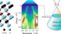
The new discovery was made in the field of Atomic Layer Deposition, or ALD for short. There are three primary ways to create and deposit thin films of various nitrides, oxides, and metals. These include chemical vapor deposition or CVD, evaporation, and sputtering. Evaporation and sputtering techniques often show poor uniformity on high aspect ratio structures such as structures with greater WDR ratios that 2. CVD tends to conform much better but unfortunately, requires immense substratal heat, and usually conflicts with gas nucleation.
ALD is a form of CVD but requires much lower temperatures which almost eliminates the issue of gas nucleation. ALD is a vapor phase technique used to produce delicate films on a multitude of substances. Reactions that occur in ALD are self-limiting and offer great conformity, as well as the control of thickness on the Angrstrom level, and alterations in the films configuration. With such potential, ALD has become a prominent apparatus in many research and industrial projects such as transistors and ALD reactors.

A diagram of Atomic Layer Deposition, courtesy of Stanford University
Currently, a “sticky” determinant precursor layer is applied to a surface where various gases are chemically bonded to form a layer of molecules which are then used in the films reaction with other elements and substances. The current molecules used to bind to the surface of the precursor layer are large enough to prevent receptors on the film to be effective, and will block the receptor points. Cadien and Muneschwar realized that the molecules would shed ions or other molecules which would use coordinate bonding to attach to the metals of the precursor layer. By the time this reaction occurred the gases contained within the chamber were already full of impurities and would have exited device.
Attempts have been made to recycle the gas used in the original reaction but are still left with impurities which could compromise the films substructure. Muneshwar then proposed that he could create a denser and more conformal layer on the film by decreasing the amount of gas within the chamber and decreasing the time between doses. This would leave enough time for the residual ligands to leave the gas molecules and unblock the precursor layer’s receptors. This realization came about as he was working as a PhD under Cadien. Muneshwar had a conversation with Cadien and one of his colleagues over the precursor costs, which are a large issue in manufacturing ALD films.
While attending an international ALD conference last year Muneshwar approached researchers and industry engineers to discuss these precursor layer costs. He asked an attendee what they would think if he was able to cut the precursor cost in half, and later ran into him again when he was told that his boss would be interested in Muneshwar’s work.
As Muneshwar arrived back at campus, he was able to create a working mathematical model that could simulate the capability of his approach. Cadien and Muneshwar then proceeded to publish their research in Journal of Applied Physics late in February 2016. They were immediately contacted by a myriad of industry leaders asking for prints of their paper.

Triratna Muneschwar and Ken Cadien, image courtesy of the University of Alberta
Only a small amount of materials used in ALD are required to create the precursor layer, however, these materials can range from 5-6 hundred dollars a gram. The current methods are destructive, and can waste between one hundred to ten thousand times the amounts of material required for a dosage in the chamber. For a large company trying to produce ten thousand components a week that require the precursor films, the cost tends to add up very quickly.
The market for high-k and ALD/CVD metal precursors is expected to hit $705.9mn by 2022 according to a study by Grand View Research. The research could prove to be an invaluable asset in the field of semiconductor production, and these metal precursors are expected to create a large shift over the forecast period as they gain an edge with their low heat and stability tract.
“There are more than 1,000 atomic layer deposition systems in the world...but there’s only a handful of people asking why and how these things work, who are trying new things. When you’re doing that, you can
come up with breakthroughs like this.” -Ken Cadien
Related Content