Facebook
 Google
 GitHub
 Linkedin
DARPA Doubles Down on Chip-Level Cybersecurity
The Automatic Implementation of Secure Silicon (AISS) program aims to make scalable security more readily available to designers.
The rise of IoT has produced countless web-accessible devices, each animated by increasingly complex, often defenseless computer chips. While this vulnerability poses threats to individual security, the risk is compounded for national security.
The Defense Advanced Research Projects Agency (DARPA) has created the Automatic Implementation of Secure Silicon (AISS) program to help lift the burden of developing secure chips. As the name suggests, this program will automate the process of securing hardware through the chips themselves.
Incorporating security directly into a chip is usually a manual task that takes time and money. It also involves trade-offs in power dissipation, size, and performance.
Serge Leef, a program manager in DARPA’s Microsystems Technology Office (MTO), says, “Today, it can take six to nine months to design a modern chip, and twice as long if you want to make that same design secure.”
DARPA's Automatic Implementation of Secure Silicon. Image used courtesy of DARPA
He goes on to explain that “While large merchant semiconductor companies are investing in in-house personnel to manually incorporate security into their high-volume silicon, mid-size chip companies, system houses, and start-ups with small design teams who create lower volume chips lack the resources and economic drivers to support the necessary investment in scalable security mechanisms, leaving a majority of today’s chips largely unprotected.”
Scalability: a Key Goal in the AISS Program
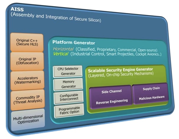
The AISS program aims to build an entire design tool and IP ecosystem to automate the process of incorporating cyberdefense into chip designs. This ecosystem will provide protection to application-specific ICs (ASIC) and SoCs from the four most threatening attacks: side-channel attacks, hardware trojans, reverse-engineering attacks, and supply chain attacks.

Core tenets of the AISS security engine. Image used courtesy of DARPA
Scalability is the key. According to Leef, the design goals of a chip, including security and economic objectives, can vary based on application. He gives the example of a chip with high security requirements that may have to settle for other tradeoffs.
“Achieving the required security level may cause the chip to become larger, consume more power, or deliver slower performance. Depending on the application, some or all of these tradeoffs may be acceptable, but with today’s manual processes it’s hard to determine where tradeoffs can be made," he explains.
The AISS design flow will seek to scale the security component of the chip to the needs of its application. Notably, AISS envisions an entirely separate partition within the chip—segregated from the chip's functional area—dedicated entirely to security.
DARPA Announces Two Teams
The AISS program includes players from the academic, commercial, and defense industries to develop DARPA's scalable security vision. Serge Leef says that AISS's top goal is to speed up the timeline—from designing the architecture to security-hardened RTL—from a year to a week.

AISS focuses on on-chip security, integration, and security tools. Image used courtesy of DARPA
DARPA recently announced the two AISS research teams:
- Synopsys, Arm, Boeing, Florida Institute for Cybersecurity Research at the University of Florida, Texas A&M University, UltraSoC, and University of California, San Diego
- Northrop Grumman, IBM, University of Arkansas, and University of Florida
Together, these two teams plan to develop an upgradable “security engine” platform that can assimilate the latest security technology as soon as it becomes available. This engine will provide the infrastructure to defend hardened chips throughout their lifecycle.
Team Objectives
Northrop Grumman and IBM will utilize DARPA’s supply chain hardware integrity for electronics defense (SHIELD) program as a starting point to develop an Asset Management Infrastructure (AMI).
AMI will be a cloud-based system that manages certificates, keys, and watermarks while also tracking data. This will help ensure that chips remain secure as they move through the design ecosystem.
Synopsys and Northrop Grumman will work on Arm devices through the modularity of the new AISS-based flows, accepting other security engines. These highly-specialized engines will be aimed for DoD applications.

Current secured-silicon development cycle for DoD applications vs. AISS secured-silicon development cycle. Image used courtesy of DARPA
Finally, Synopsis will lead an effort to merge the AISS-developed electronic design automation (EDA) tools with commercial off-the-shelf IP from Synopsys, Arm, and chip instrumentation specialist UltraSoc. The resulting solution may empower chip designers to specify power, area, speed, and security (PASS) constraints.
Democratizing Chip-Level Security
DARPA recognizes that hardware security is a specialized discipline mostly dominated by huge merchant semiconductor companies, such as Qualcomm, Intel, and Broadcom. Through automation, DARPA hopes to democratize the process of building chip-level security, making it an achievable goal for even the smallest of IC builders.
Have you ever worked with hardware security? What challenges did you face? Share your experiences in the comments below.
Related Content