Facebook
 Google
 GitHub
 Linkedin
From Laser to Workbench: New Tech Speeds Up PCB Solder Mask Production
A new laser direct imaging technology may significantly increase the speed of solder mask production at a low cost.
The solder mask is a PCB's first line of defense against degradation from corrosion and oxidation. The solder mask also acts as a layer of protection between solder joints and other conductive materials on the PCB, preventing bridges from forming during the assembly process.

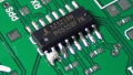
Solder mask close-up. Image (modified) used courtesy of Tempo Automation
Unfortunately, the solder mask manufacturing process poses some challenges that can hinder the production efficiency of PCBs.
The Solder Mask Manufacturing Process
Solder mask is made up of a polymer layer that coats over the metal traces of a board. As mentioned, the solder mask is crucial to the longevity of a board. As such, it is imperative that the solder mask is applied reliably for the end device to operate.
According to Tempo Automation, some popular forms of application include:
- Screenprint (recommended for thin cores and flexible substrates)
- Curtain coat
- High-pressure, low-volume (HPLV) air spray
- Electrostatic spray
Nowadays, solder masks are typically manufactured using a direct imaging (DI) technique, which is necessary to comply with registration and accuracy requirements. These techniques generally consist of applying ink to the surface of the PCB and curing it with UV lights to form the hardened mask.
Shortcomings of Direct Imaging
One issue posed by solder mask manufacturing is that the inks require significantly higher doses of ultra-violet (UV) energy than dry-film.

Direct imaging solder mask application. Image used courtesy of Limata
Because of this, the imaging processing times of DI solutions that solely rely on UV-light sources are often too slow for high-volume requirements or fail to deliver the required solder mask (SM) imaging output capacity at a reasonable investment for the manufacturer.
Limata Combines UV and IR Laser Power
Last week, Limata announced a new technique that they claim significantly increases solder mask production efficiency at a lower cost to the manufacturer.
This technology, called LUVIR, tackles the aforementioned problem by using a combination of UV and IR laser power. The technique consists of using the IR light to heat up the ink directly before the UV laser starts curing the ink. The addition of this heat makes the solder mask more reactive with the UV light, significantly reducing the UV power necessary to cure the mask.

Depiction of the LUVIR X3000 technology. Image used courtesy of Limata
The result is a faster and more efficient process.
This technology is also versatile. Limata explains on their website that “Higher capacity levels with LUVIR are particularly achieved on all conventional solder mask ink types and colours (i.e. green / black) requiring high-UV energy doses between 400–1,000 mJ/cm2, and accounting for ca. 90% of the total inks used in the standard PCB solder mask process.”
Improved Solder Mask Processes Help Everyone
Sometimes improvements in manufacturing can be just as important as improvements in device technology. With faster time to market and cheaper production costs, engineers can provide consumers with new technologies quicker and at lower costs than before.
Any way you look at it, new technology for solder mask manufacturing will certainly bring about a slew of benefits for everybody—from the engineer to the consumer.
Related Content