Facebook
 Google
 GitHub
 Linkedin
Infineon’s Rad-Hard GaN Transistors Cleared for Space and Defense
Fabricated at Infineon’s own foundry, the GaN transistors are the first to earn the highest certification of reliability by the U.S. Defense Logistics Agency.
Infineon recently released the industry's first radiation-hardened GaN power transistor to receive full qualification under the United States Defense Logistics Agency’s Joint Army-Navy Space (JANS) Specification MIL-PRF-19500/794. Infineon is among the few companies with in-house GaN fabrication capabilities to meet the highest reliability standards.

Infineon built its radiation-hardened GaN transistors for on-orbit space vehicles, manned space exploration, and deep space probes.
All About Circuits heard from Infineon’s Josemari Mapa, product marketing engineer, and Sean Darcy, senior director of aerospace and defense, about this qualification and its implications.
TID and SEE Qualification
JANS qualification establishes compliance with rigorous screening and quality protocols that confirm a device's resilience in extreme space environments. These include single-event effects (SEE), total ionizing dose (TID) exposure, and thermal-mechanical integrity under prolonged mission conditions.
Infineon’s JANSG2N7697UFHC and its commercial equivalents, the IG1NT052N10R and IG1NT052N10G, were subjected to comprehensive radiation testing to validate their robustness. Specifically, all three devices are rated for a total ionizing dose tolerance of 500 krad(Si), with testing conducted at a dose rate of 173 rad/s using Cobalt-60 gamma sources.
“This milestone brings GAN technology to the space power community while extending and complementing Infineon's position based on our industry-leading, radiation-hardened silicon MOSFETs,” Darcy said.
Throughout the testing, and across multiple devices from separate wafer lots, no significant shifts were observed in parameters such as gate leakage (IGSS), drain-source on-resistance (RDS(on)), or threshold voltage (VGS(th)).
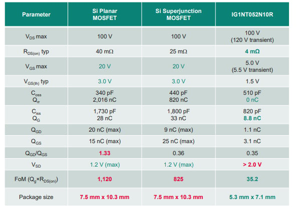
A comparison of radiation-hardened FETs.
In terms of single event effects, the GaN devices demonstrated tolerance up to a linear energy transfer (LET) of 70 MeV·cm2/mg using gold ions. That corresponds to an LET(Si) equivalent of 86.5 MeV·cm2/mg, which places the parts well above the SEE performance thresholds typically encountered in geostationary or deep space radiation belts. Notably, the devices passed both catastrophic and parametric SEE tests across three wafer lots.
“The GaN part is usable up to its full capability and requires no derating up to its maximum gate-to-source and drain-to-source voltages,” Darcy explained.
Architectural Advantages of GaN Over Silicon
GaN HEMTs offer material-level and structural advantages over silicon devices for radiation tolerance.
For example, GaN devices in lateral HEMT configurations benefit from a 2D electron gas (2DEG) channel formed at the GaN/AlGaN heterojunction. This channel enables extremely high electron mobility and supports faster switching speeds with significantly lower conduction losses.
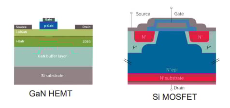
GaN HEMT versus Si MOSFET device structure.
Infineon’s IG1NT052N10R features a typical RDS(on) of 4 mΩ and a total gate charge (QG) of 8.8 nC. The figure of merit, defined as QG × RDS(on), is 35.2 nC·mΩ, representing a significant improvement over the 825–1120 nC·mΩ range typically observed in radiation-hardened silicon alternatives. The device also exhibits zero reverse recovery charge (QRR). In contrast, comparable silicon superjunction devices exhibit QRR values exceeding 800 nC. GaN HEMTs also benefit from an inherent lack of a gate oxide layer.
“Due to the material structure of GaN, the lack of the gate oxide eliminates the failure mechanism that's normally seen with a silicon FET,” Mapa said.
This inherent immunity to TID-induced oxide degradation makes GaN a more stable platform for extended exposure missions.
Packaging and System-Level Integration
Infineon’s new transistors are housed in a novel flip-chip ceramic package dubbed PowIR-SMD, which was developed specifically for high-reliability GaN. Compared to the standard SMD-0.5 package, PowIR-SMD achieves a 49% smaller footprint and a 97% lowered inductance, measured at just 0.1 nH. Such a low parasitic profile directly contributes to faster switching transitions and improved EMI performance.
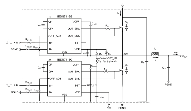
The new GaN devices are configured with the 1EDN7116G gate driver.
The devices are also compatible with Infineon’s EiceDRIVER 1EDN7116G gate driver and are available on a reference half-bridge evaluation board. The board supports input voltages up to 80 V and includes dead-time generation. Efficiency benchmarks show up to a 9.4% gain over traditional 100-V MOSFETs in synchronous buck topologies operating at 200 kHz.
A Straight Roadmap to Availability
With this release, Infineon becomes the first vendor to offer JANS-qualified GaN devices built entirely in-house, with full control over epitaxial growth, wafer processing, assembly, and testing. According to Infineon, this vertical integration will be invaluable in securing long-term supply chains for aerospace and defense contractors concerned with geopolitical supply risks or single-source dependencies. Evaluation boards and engineering samples are already available, and production volumes for the JANSG2N7697UFHC are expected to ramp by summer 2025.
All images used courtesy of Infineon.
Related Content