Facebook
 Google
 GitHub
 Linkedin
Inside eMASS’s ECS-DoT SoC: Decompression and AI at the Sensor Edge
In this exclusive CES interview, All About Circuits learned how EMASS's new ultra-low-power SoC brings intelligence where size, power, and latency matter most: the sensor edge.
EMASS arrived at CES with a clear message about where they believe edge AI architectures are headed. Rather than scaling performance through higher clock rates or larger cores, the company is betting on aggressive data reduction and dense on-chip memory to push inference closer to the sensor under extreme power constraints. EMASS's approach to that strategy is its new ECS-DoT SoC.
At CES 2026, we spoke with EMASS CEO Mark Goranson, along with other company representatives Shantanu Rakoe and Scott Smyser, to learn how ECS-DoT approaches the sensor-edge problem differently from conventional microcontroller and edge AI platforms.

Left to right: EMASS’ Amidom Giday, Mark Goranson, CEO of EMASS, Shantanu Rakoe, VP of Systems Design and Engineering, and Scott Smyser, VP of Sales and Marketing at CES 2026.
A Sensor-Adjacent Architecture
At the highest level, EMASS designed ECS-DoT as a sensor-edge device rather than a general-purpose application processor.
“Our focus is what we call the micro or sensor edge,” Rakoe explained. “Sitting next to sensors in battery-constrained devices, doing always-on inference with very low latency and very low energy consumption.”
Instead of relying on external DRAM or cloud offload, EMASS designed ECS-DoT to execute complete AI workloads locally. To that end, the SoC integrates a 32-bit RISC-V core alongside dual deep-learning accelerators, dedicated DMA, and 4 MB of on-chip memory split evenly between SRAM and MRAM.
Fabricated on a 22 nm process, the device targets continous inference workloads that operate between 0.1 mW and 5 mW, with inference latency under 10 ms. Meanwhile, standard interfaces such as I2C, SPI, QSPI, CPI, and GPIO enable direct attachment to cameras and sensors without a host processor in the loop.
The Decompression Engine
The most distinctive element of ECS-DoT’s architecture is its proprietary on-chip AI weight decompression engine. EMASS compresses neural network weights offline to as little as two bits per parameter, with typical averages near 1.3 bits per weight. At runtime, those weights are decompressed back to 8-bit precision before execution on the accelerators.
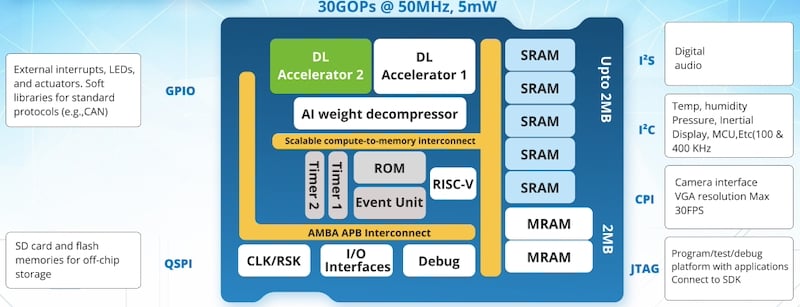
Block diagram of the ECS-DoT. Image used courtesy of EMASS
“Our secret sauce is the deep learning accelerators and the decompressor on the chip,” Rakoe said. “You store models at two or four bits per parameter, but at runtime you get the accuracy of eight bits.”
Unique to EMASS, this approach allows significantly larger models to reside entirely in on-chip memory or external flash while maintaining inference accuracy. The decompressor operates in tandem with QSPI flash, enabling high-bandwidth models to stream without the energy penalties typically associated with external memory access. According to EMASS, this compression-first architecture directly reduces memory size, access energy, and inference latency.
MRAM for Non-Volatile Storage
MRAM is part of ECS-DoT’s ability to operate independently of external memory. The SoC integrates up to 2 MB of MRAM alongside 2 MB of SRAM, allowing non-volatile storage of compressed models, firmware, and inference data.
“Part of our claim to fame is that we can do everything on board,” Smyser said. “We don’t have to access the cloud, and we don’t have to pull data from external memory.”
While MRAM scaling is proving challenging at advanced nodes, EMASS selected MRAM for this generation to enable full on-device execution and rapid wake-up behavior. The company indicated that future devices will transition to alternative non-volatile memory implementations to support further process scaling.
Dual Accelerators and Power Gating
ECS-DoT runs inference exclusively on its two custom-designed, deep-learning accelerators. The RISC-V core orchestrates control flow, peripheral management, and event handling, but it is power-gated during inference execution. This separation avoids the inefficiency of running neural workloads on a general-purpose processor.

EMASS’s Shantanu Rakoe, VP of systems design and engineering, demonstrates ECS-DoT in a wake-word detection scenario at CES 2026.
“A lot of competitors put AI on the main processor and keep that processor spun up all the time,” Smyser said. “We do AI exclusively on the accelerators and power-gate everything else.”
While AI inference is running, EMASS applies power gating across unused memory banks, peripherals, and compute blocks, including MRAM when it is not required. Such granular control reduces active energy consumption to as low as 1 µJ to 10 µJ per inference, depending on the workload.
At CES, EMASS referenced MLCommons benchmarks to contextualize ECS-DoT’s performance. For tasks like image classification and visual wake-word detection, the company claims energy consumption up to 20x lower than competing ultra-low-power AI platforms and orders of magnitude lower than microcontroller-based implementations. Specifically, ECS-DoT delivers up to 30 GOPS at 50 MHz while consuming roughly 5 mW, translating to an efficiency of approximately 12 TOPS/W.
“A lot of companies claim ultra-low power, but we’re ultra-low power when we’re actually doing the work,” Rakoe said. “That’s what matters.”
Production and Roadmap
ECS-DoT is scheduled for mass production in Q2 2026, with multiple OEM evaluations underway. EMASS also previewed a follow-on device fabricated on a 16-nm process that adds Bluetooth Low Energy, enhanced vision acceleration, and expanded numerical precision.
For now, ECS-DoT establishes EMASS’s architectural thesis. By treating compression, decompression, and dense non-volatile memory as primary design elements, the company is redefining how much intelligence can live at the sensor edge without sacrificing accuracy, latency, or battery life.