Facebook
 Google
 GitHub
 Linkedin
Intel Showcases a Photonics “First” — an Eight-wavelength Laser Array
Intel Lab researchers push photonics one step further by demonstrating a tightly controlled, highly integrated eight-wavelength laser.
The field of integrated photonics has increased in importance significantly in the past decade. Where trends like rising data rates and traffic are increasingly limiting the performance of conventional copper interconnects, photonics and integrated photonics have become crucial to networking infrastructure.
Intel has invested heavily in photonics through its Intel Labs. With that in mind, it recently has been met with an industry first in integrated photonics thanks to the demonstration of a tightly controlled, highly integrated, eight-wavelength laser.

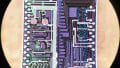
Illustration of 8 micro-ring modulators and the optical waveguides. Image used courtesy of Intel
Recently, All About Circuits had the opportunity to talk with James Jaussi, Senior Principal Engineer and Director of the PHY Research Lab at Intel Labs, and Dr. Haisheng Rong, Sr. Principal Engineer with Intel Labs, to hear more about the announcement.
The Need for Photonic Integration
As the electronics industry trends towards faster data rates and smaller node sizes, many concerning trends are confronting the field.
One of these trends is the rise of electrical interconnects performance limitations due to a coupling of the non-idealities of copper with increasing frequencies, leading to more parasitic. As Jaussi explains:
“One motivation for looking at optical and optical communication is looking at where things are for the electrical interfaces. As performance has been increasing on a per-package basis over time, the total power of the package has been increasing. But the rate of power increasing for the I/O or the interface to escape out from the package is increasing at a faster rate.
What this illustrates is the importance and the trade-off that is occurring right now: as the I/O power does not scale as quickly as the increase in power-per-package scales, there's a point at which those could cross over and this is can be referred to as a power wall.”
To many, the path towards future I/O interfaces with improved energy efficiency and longer reach may very well be integrating silicon circuitry and optics side by side on the same package. By combining CMOS and photonics into a single package, researchers believe that they could directly address the limitations of conventional copper interconnects to increase overall bandwidth, energy efficiency, and circuit complexity.
Integration for Multiwavelength Lasers
One important photonic application that stands to benefit from high integration is that of the multiwavelength laser.
In communication applications like the internet, the most simple form of optical communication is with a single fiber consisting of a single wavelength laser TX/RX scheme. However, in practice, engineers will put an array of lasers, each composed of different wavelengths, as the bandwidth requirements increase, into a single fiber. Today, long-haul communication systems can have almost 100 wavelengths utilized in a single fiber.
However, this kind of scheme becomes very hard to achieve when it comes to chip-to-chip communications. As Rong explains:
“When we’re talking about chip-to-chip communications, we require a lot of components, literally billions of components such as separate lasers and modulators. Ultimately, the cost is prohibiting when we are using traditional technology. Integration is going to be key for moving forward, and we have identified early on that silicon photonics technology would enable that.”
To achieve the integrated photonics necessary for chip-to-chip communications, Intel Labs has explored co-packaged optics solutions using dense wavelength division multiplexing (DWDM) technology. This strategy has shown the promise of increasing bandwidth while significantly reducing the physical size of photonic chips. However, a major challenge thus far has been how to produce DWDM light sources with uniform wavelength spacing and power.
Intel's Integrated Eight-wavelength Laser
Today, Intel made significant advances in the field with the announcement of a successful demonstration of a tightly controlled, integrated eight-wavelength laser.

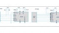
Illustration of 8-channel hybrid III-V/silicon distributed feedback (DFB) laser array. Image used courtesy of Intel
The optical solution is a distributed feedback (DFB) laser array that is fully integrated on a silicon wafer and was designed and fabricated on Intel's 300 mm hybrid silicon photonics platform. Within this, Intel used advanced lithography to define the waveguide gratings in silicon prior to the III-V wafer bonding process, allowing for better wavelength uniformity compared to conventional semiconductor lasers. As Rong explains:
“We accomplished this laser area with eight lasers with very uniform wavelength spacing, which is really hard to achieve. We have unique design and fabrication technology that allows us to do what nobody else can. We bound a very small piece of phosphate chip on the wafer and we planarized and removed the substrate fab. The result was a wafer with a very thin film of the phosphate on it.”
The result is a laser array that promises to deliver an impressive output power uniformity of +/- 0.25 dB and wavelength spacing uniformity of ±6.5%, exceeding industry specifications.
Moving forward, Intel believes its advancement will be instrumental in facilitating network-intensive workloads, including artificial intelligence and machine learning.
Interested in other photonics-related innovations? Read on in the articles down below.
Harvard Kicks Photonics Up a Notch With First Integrated Laser on TFLN Chip
Photonic Wire Bonding Process Could Open Door to More Photonic Electronics
Salience Labs Marries Photonics and Electronics in AI Processor