Facebook
 Google
 GitHub
 Linkedin
Single-Photon Avalanche Diodes (SPADs) Swerve Breakdown Voltage and Buoy Photonics
SPADs, a branch of photodetectors, are leading the way in photonics innovation.
A single-photon avalanche diode (SPAD) is a class of photodetectors that can detect low-intensity signals down to a single photon. Similar to avalanche photodiodes (APDs), SPADs exploit the photon-triggered avalanche current of a reverse-biased p-n junction to detect incident radiation.
The study of photonics has one underlining challenge: detecting a single photon. For decades researchers have attempted to create a one-stop-shop for photon sensing, looking to SPADs as the foundation.
SPADs Compared to Regular Diodes
Diodes are essentially switches that allow current to easily flow in one direction while resisting current flowing in the opposite direction. SPADs were designed to operate in reverse bias and can continue to operate at higher voltages than standard reverse-biased diodes. The anatomy of SPADs is similar (and distinct) from that of diodes.

Diagram of a reverse-biased diode. The depletion region begins to expand as it resists current until the voltage reaches the breakdown stage, at which the diode will collapse. Image used courtesy of Tony R. Kuphaldt
A standard diode in reverse-biased will experience breakdown and burned components, a phenomenon caused by a voltage exceeding its peak inverse voltage. Most rectifiers or reverse-biased diodes will only be able to handle around 50 V at room temperature. If the temperature rises, so too does voltage rise, speeding the rate at which breakdowns occur.
SPADs are unique because they can continue to operate past the breakdown voltage.
The Constraints of SPADs: Temperature and Fabrication
Like any other device, SPADs have their limits. First, the breakdown voltage is strictly dependent on the temperature of the p-n junction. If temperatures have an extreme rise, then the device meets its breakdown voltage sooner. Even though SPADs can handle more voltage, placing SPADs in harsh conditions may still cause burnout to occur.

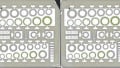
Examples of SPAD-integrated devices. Image used courtesy of the SPAD Lab
Another limitation is present in the fabrication processes; when developing the structure of the SPAD, a facility must be stringent on preventing contamination. Crystal defects can cause afterpulsing, a non-ideal behavior of SPADs that jeopardizes any application that counts the number or timing of detection events—which is the intended nature of SPADs in the first place.
SPADs as a Candidate for Photonics
SPADs are widely used for their versatility in photonics since they are sensitive enough to detect single photons while consuming low amounts of power.
There are two types of SPADs: thin and thick junction. Thin junction SPADs operate at 10 V to 50V and are designed for low-power dissipation design constraints.

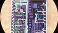
Diagram of a SPAD's structure along with an array layout. Image used courtesy of the Catania Astrophysical Observatory Laboratory for Detectors
Thick junction SPADs are able to operate at much higher breakdown levels, 200 V to 500 V, for high-power dissipating designs. SPADs are especially useful for LiDAR, medical imaging, and any other application where light is focused on a small region.
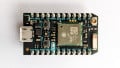
ST's New Time-of-Flight Module Taps into SPAD Arrays
As an example of recent innovations in SPAD technology, ST recently announced what it claims is the industry's first 64-zone direct time-of-flight module, the VL53L5 ToFsensor. This sensor features a 940 nm vertical cavity surface emission layer (VCSEL) light source, an SoC sensor with VCSEL driver, a low-power 32-bit MCU core, and—importantly—an array of receiving SPADs.
The architecture of the new module design includes both transmit and receive lenses. As mentioned previously, ST says the device is able to gather ranging data from up to 64 zones. The company also says the device is widely applicable thanks to an array of receiving SPADs with controllable zone parameters with each zone having an output frame rate of 60 fps.
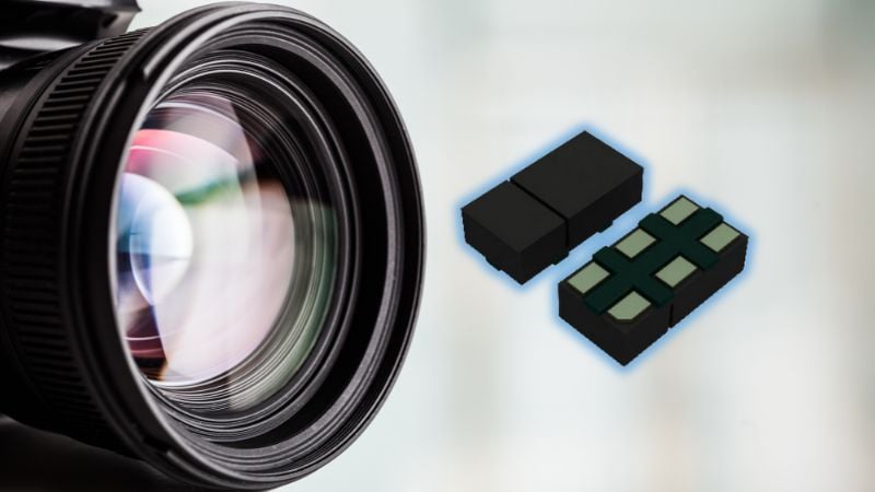
The ability of a ToF sensor to detect multiple targets and reject reflection can improve smartphone/camera performance.

Examples of electrical schematics using the VL53L5. Image used courtesy of STMicroelectronics
General Manager of ST’s Imaging Division Eric Aussedat shared insight into the structure of the new sensor: “The multi-zone VL53L5 FlightSense direct Time-of-Flight sensor uses our most advanced 40nm SPAD production process to offer outstanding 4m ranging performance and up to 64 ranging zones that help an imaging system build a detailed spatial understanding of the scene.”
Eric Aussedat also discussed the importance of the SPAD-based sensor toward imaging capabilities, explaining that the device delivers 64 times more ranging zones than predecessors. With these features in mind, the VL53L5 was designed to improve laser autofocus, presence detection, gesture interfaces, touch-to-focus, and other imaging technologies.