Facebook
 Google
 GitHub
 Linkedin
Fast Screening for Next-Gen Memory Chips: A Look at Intermolecular, a Silicon Valley Fab Company
Here is the profile of a fab that provides composition screening and stack engineering services for new materials used in the next-generation memory devices.
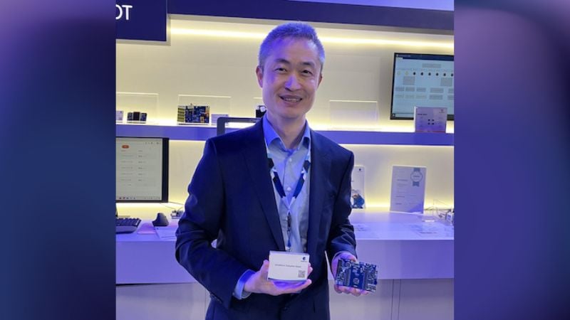
AAC's Majeed Ahmad was able to visit the facilities of Silicon Valley-based fab services company, Intermolecular Inc. (IMI). Here is a profile of a fab that provides composition screening and stack engineering services for new materials used in the next-generation memory devices.
A fab in Silicon Valley. Really? There is a foundry in the heart of the tech valley that claims to accommodate the data explosion and the need for higher speeds in the next-generation memory designs. Intermolecular Inc. (IMI), headquartered in San Jose, California, specializes in outsourced R&D services for materials used in memory products.
The fab services company, founded in 2004, is focusing on the highly-fragmented memory market. IMI serves Tier 1 integrated device manufacturers (IDMs), foundries, tool makers and material suppliers for DRAM, ReRAM and PCRAM chips. The company is also making a foray into the NAND flash-related services.
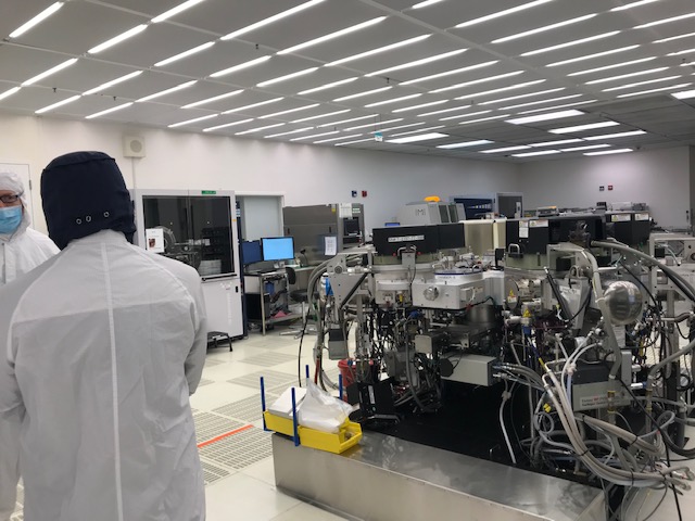
Unlike traditional semiconductor fabs, optimized for manufacturing, IMI’s processes are optimized for materials understanding. Image courtesy of Intermolecular.
The potential for new materials in memory chips is exploding, but at the same time, the materials-related innovations are costly and complex. What IMI does is handle these complex and toxic materials by enabling fast screening while minimizing the fab exposure to contamination.
“It’s an exciting time for materials and materials engineering,” says Ellie Yieh, VP and GM of Advanced Product Technology Development at Applied Materials, noting solving that the major challenges that face this field require new materials.
Each of the potential memory technologies has a unique material set associated with the process and performance development. The deposition of these materials or combinations of materials is typically completed by the atomic layer deposition (ALD) or physical vapor deposition (PVD) workflows for semiconductor memory applications, which is at the heart of IMI’s business.
Read More:
- As Emerging Technologies Outpace Semiconductor Processes, IBM Takes Leap Towards 7nm IC Fabrication
- Could Molecular-scale ALD Revolutionize Electronics Manufacturing?
- Competition for 7 nm Chips: Intel, AMD, and the Shift of Chip Manufacturing to TSMC
Support for DRAM and Flash Materials
Take DRAM chips as an example, which require dielectrics composition screening to improve the high-k. IMI facilitates the screening of interfacial layers and offers material and process development services to tune work function contacts to further reduce dielectric thickness.
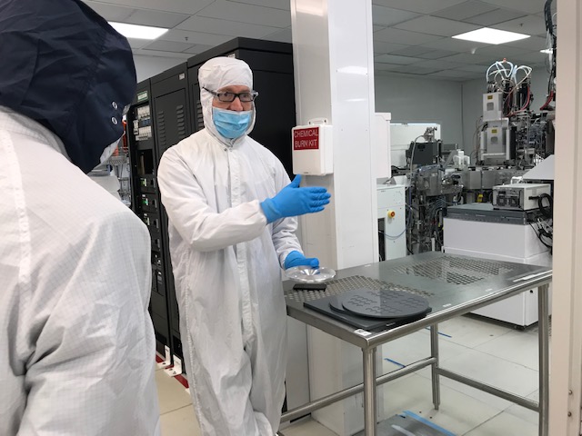
IMI provides high-throughput experimentation for composition screening and stack engineering to ensure greater density, speed, and endurance of memory devices. Image courtesy of Intermolecular.
Next, take the example of 3D NAND flash chips, which have leapfrogged from 72-layer stacks to 256-plus layers. Inevitably, while the layers are getting thinner, the stacks must be designed differently, making interfaces far more critical.
In August of last year, AAC's Chantelle Dubois interviewed Toshiba's Senior VP of Memory Business, Scott Nelson, and his colleague on the technical team, Doug Wong, about this very concept. Toshiba's approach to stacking memory has been to move into the realm of 3D, developing proprietary BiCS ("bit column stacked") technology to achieve the then-high 64 layers.
For their part, IMI aims to help chipmakers improve the reliability of memory cells by providing lower-resistivity metals for word-line metallization. The company also offers the precursor and dielectrics/charge trapping layer screening for higher aspect ratios.
Efficient Processes, Efficient Memory
There is also an explosion of data amid the arrival of new materials and higher throughput demands in memory designs. So, the materials specialists like IMI are combining the data with machine learning expertise to de-bottleneck every step in the materials screening. As a result, engineers don’t have to spend four to five hours in gathering data.
The profile of IMI, a fab services company, shows how it delivers validation of materials for memory products with greater throughput, faster R&D cycles, and lower risks to new materials introduced in the fab. In other words, IMI operates on the principle that test structures for new materials can be implemented faster while making the learning cycles as short as possible.
With the NAND flash memory shortage only recently abating, increased efficiency in every step of memory chip evolution—from research on materials to fabrication, itself—is noteworthy.
Do you have experience with applications that demand ever-increasing amounts of memory? What's your experience with memory fabrication? Share your thoughts in the comments below.
Related Content