Facebook
 Google
 GitHub
 Linkedin
Microchip Clock Buffers Bridge SoCs & FPGAs With Higher-Voltage Sources
The SY757xx family translates clock inputs from 1.2 to 3.3 V down to 1.2 V LVCMOS outputs at frequencies up to 250 MHz,
Microchip Technology recently announced a new family of LVCMOS clock buffers to drive 1.2 V outputs for FPGAs, SoCs, and CPUs. Dubbed the SY757xx family, these new devices are meant to offer a simple, reliable way to translate conventional board-level oscillator and PLL outputs to lower-level voltages. According to Microchip, they offer a marked improvement over conventional approaches to clock voltage scaling, such as voltage dividers.
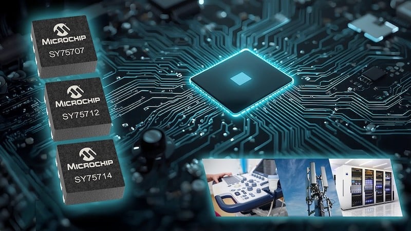
Microchip’s SY757xx family of 1.2V-output LVCMOS clock buffers. Image used courtesy of Microchip.
The SY757xx Family
Microchip designed the SY757xx family to improve clock fanout at relatively low 1.2 V rails, where edge uncertainty becomes more pronounced and margin for error shrinks. Spanning 11 parts that handle voltage translation and clock fanout in a single package, the new device family covers 0 Hz to 250 MHz and accepts translation inputs from 1.2 to 3.3 V. According to the company, additive jitter within the family reaches as low as 26 fs.
An example within the family is the SY75707, which takes a single differential input and drives two LVCMOS outputs. It accepts 1.8 to 3.3 V on VDDIN while powering the output stage from a 1.2 to 1.8 V rail. Microchip specifies 32 fs typical additive RMS jitter in the 12 kHz to 20 MHz band with a 156.25 MHz clock, alongside a noise floor of −165.3 dBc/Hz. Skew between the two outputs stays under 50 ps, and the input-to-output delay runs at 1.2 ns typical. More information is available in the SY75707 data sheet.
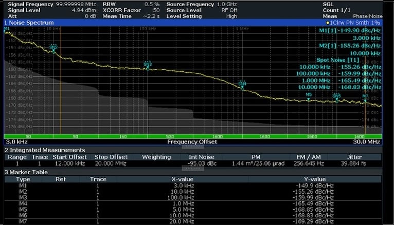
Clock output phase noise of the SY7570x. Image used courtesy of Microchip.
Because the part targets green servers and battery-powered designs, Microchip held current draw to 4.8 mA on VDDIN at 3.3 V and 3.9 mA on the 1.2 V output rail. The buffer passes spread-spectrum modulation through untouched, operates from -40 to +105°C, and occupies a 1.4 x 1.6 mm VDFN package.
Other family solutions, like the SY75712 and SY75714, extend the same approach to wider fanout, driving two and four outputs from a 1.2 to 1.8 V supply in 2 x 2 mm TDFN packages.
Shortcomings of Voltage Divider Translation
Advanced logic processes continually reduce I/O supply voltage, with JEDEC codifying the 1.2 V interface levels as of 2007. However, clock sources have not scaled at the same pace. Crystal oscillators, PLLs, and jitter cleaners still operate at 1.8 and 3.3 V, meaning any design pairing a high-density logic device with a conventional timing chain needs a translation stage between them.
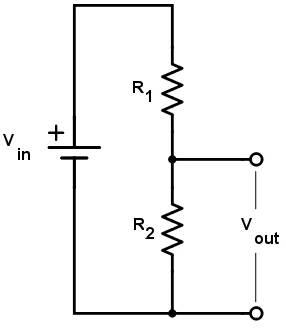
Simple voltage divider circuit. All About Circuits image.
The simplest translation stage is a resistive divider, which scales the clock amplitude but also the slew rate. Additionally, the divider’s source impedance often combines with the receiver's input capacitance to form a low-pass pole that further rounds the edges. Slower edges widen the window in which the receiver decides where the transition occurred, so noise riding on the clock converts more readily into timing error.
This approach also suffers from threshold drift. A divider sets a fixed attenuation ratio, so the clock's crossing point relative to the receiver's switching threshold moves with temperature and supply tolerance. Once that crossing point drifts off center, the clock's high and low intervals stop matching, and duty-cycle distortion appears at the receiver even though the source may have produced a clean waveform.
SY757xx Availability and Pricing
As of today, Microchip has the SY75707TWL-TR, SY75712TWL-TR, and SY75714TWL-TR in volume production, priced from $0.50 to $0.83 per unit in quantities of 10,000. The remaining eight members are sampling in limited volumes, all in 8-pin VDFN packages.