Facebook
 Google
 GitHub
 Linkedin
Nanusens Reimagines MEMS Fabrication—With Major Capacitance Payoffs
By modifying CMOS processing techniques, Nanusens claims to have made a breakthrough in MEMS sensor fabrication.
Microelectromechanical systems (MEMS) are developed using meticulous semiconductor fabrication techniques. Several semiconductor companies specialize in fabricating MEMS ICs for accelerometers, gyroscopes, pressure sensors, and more.

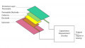
Schematic diagram of a MEMS structure in CMOS. Image used courtesy of Nanusens
U.K.-based Nanusens, a company specializing in making nanosensors inside CMOS, is now innovating novel techniques to fabricate MEMS ICs. The company’s MEMS-in-ASICs sensor technology recently bagged an IP licensing agreement with Azoteq, a developer of high-volume sensor fusion ICs. This agreement enables Nanusens to expand its MEMS-in-ASICs sensor technology in 3D accelerometers.
Challenges in MEMS Fabrication
MEMS devices are usually fabricated using two dice: one from a CMOS wafer and the other from a MEMS wafer. This two-dice manufacturing process poses several challenges for manufacturers. It's expensive to produce separate wafers for MEMS and CMOS, it extends the time-to-market, and it only produces small batches (especially in case of silicon shortages).

Nanusen recently secured its first IP license for its MEMS-in-ASICs sensor technology. Image (modified) used courtesy of Nanusens
Some companies are trying to work around these challenges by building MEMS wafers on an existing CMOS wafer. While this process might improve performance and reduce parasitic capacitance for a single MEMS sensor, it can’t be used to manufacture MEMS devices that pack multiple sensors together in a single IC. In other cases, companies might use CMOS fabrication techniques for MEMS fabrication. For instance, some developers have resorted to using the materials existing in the back end of line (BEOL) of the CMOS processing to fabricate MEMS.
Nanusens' CMOS-for-MEMS Technique
Nanusens has successfully fabricated a MEMS chip that boasts a reduced cost and size of about 1 mm3 (1 cubic millimeter). The company developed this chip by leveraging a vapor hydrofluoric (vHF) etching technique in the BEOL of a CMOS process. According to Nanusens, the intermetal dielectric (IMD) is etched away through the pad openings in the passivation layer. vHF is then used to create nanosensor structures. By employing 0.18-micron CMOS technology, the company claims it can massively scale the production of the MEMS chip.

Close-up view of two MEMS sensors in a single ASIC chip. Image used courtesy of Nanusens
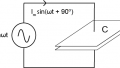
The vHF technique helped reduce the parasitic capacitance between the top and bottom metal planes of the device. This reduction of the parasitic capacitance (about 50 fF) is said to increase sensitivity and performance. With the success of this single MEMS sensor chip, Nanusens aims to now combine several MEMS nanosensors on the same chip using the vHF technique.
Use in Consumer Device Motion Detection
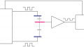
Thanks to a ring oscillator in the device, the device provides capacitance sensing; a change in the value of capacitance signifies changes in movement. The ring oscillator in the capacitance sensor eliminates bulky components like analog-to-digital converters, analog filters, and so on. Designers may adopt the sensor as a motion sensor for movement detection in smartphones, wearables, and other consumer electronic devices.
Related Content