Facebook
 Google
 GitHub
 Linkedin
“World’s Smallest” GaN Laser Chip to be Mass Produced on Silicon Substrate
A new GaN laser chip from Kyocera may shine a path forward for low-cost, high-yield optoelectronics chips on silicon substrates.
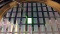
Marking a significant milestone in the continued miniaturization of optoelectronics, Kyocera recently announced a novel gallium-nitride (GaN) laser chip grown on a silicon (Si) substrate. This newly created chip is among the smallest laser sources to be produced on Si and is possible thanks to a new GaN growth process from Kyocera.
In addition to the raw merit of a laser smaller than 100 µm, the advances from Kyocera indicate a larger trend further uniting the fields of optics and electronics. Laser and fiber optic technology has already offered designers new methods of high-speed communication. Increased integration for future optoelectronics devices offers unwarranted flexibility and interoperability between the optics and electronics fields.

100 µm long laser developed by Kyocera, highlighting the new processes' ability to produce small optoelectronic devices. Image used courtesy of Kyocera
In this article, we'll examine Kyocera's announcement alongside other laser-on-chip technology to understand the motivation and methods to miniaturize optoelectronics further.
Improving the Yield of GaN on Silicon
One of the major hurdles for GaN optoelectronics devices is the relatively young age of device fabrication techniques. When compared with well-known CMOS processes, the methods by which GaN devices are grown are still new and semi-experimental. In a typical scenario, the GaN device may be grown on a sapphire or GaN substrate, then “peeled” off to isolate the device itself.
This process comes with inherent drawbacks, the first of which is cost. GaN growth typically requires expensive substrates, while cheaper Si substrates cannot be used due to the difficulty of peeling. In addition, growing GaN on sapphire increases the number of defects due to lattice incompatibility. Finally, the physical act of peeling can often damage the device, creating high degrees of process inefficiency.

GaN growth process using an opening to create a channel of GaN. GaN is then grown laterally, allowing for a higher yield with fewer defects. Image used courtesy of Kyocera
To resolve these issues, Kyocera researchers developed a new process that doesn’t rely on expensive materials and can simplify the peeling process. Beginning with a silicon substrate, Kyocera formed a small GaN layer. The researchers then deposited a non-growing mask on the top of the wafer with an opening. Through this opening, GaN may grow. The GaN grown over the opening still includes defects since growth does not occur on the mask. GaN grows laterally from the opening, creating high-quality GaN on a less expensive substrate while isolating defects to a small area. With this process, peeling becomes trivial due to the isolation provided by the mask.
The Race to Smaller and Faster
Researchers from Kyocera have applications in mind for the newly created optoelectronic devices. Efficient micro-light sources may be used in applications requiring small, bright illumination, such as autonomous transportation. In addition, new GaN laser sources can be used in many fields such as imaging or high-speed communications.

Microcomb generated by an on-chip system. Each wavelength component may be modulated to create numerous information streams. Image used courtesy of UCSB
Kyocera is not alone in innovating optoelectronics. In July 2021, researchers from the University of California Santa Barbara developed a highly scalable laser and microcomb, capable of increasing the available communication channels for an optical system while maintaining the scalability of a single-chip solution. Building on this work, a study published in Nature Photonics revealed single-chip communication speeds up to 1.84 Pbit/s with a theoretical target of 100 Pbit/s.
The Future Looks Bright for Optoelectronics
Optoelectronics is forging ahead in the effort to build smaller, more scalable devices with little impact on overall performance.
The new GaN growth process from Kyocera, coupled with scalable designs demonstrated in academia, could mark the beginning of an overhaul from electric to optic-based communications systems. In addition, the ability to seamlessly include optics devices on-chip gives designers another tool to use when developing the next generation of integrated devices.