Facebook
 Google
 GitHub
 Linkedin
New Quantum Image Sensing Tech Trumps Traditional Image Sensors
CMOS imaging loses 75% of incident light. Quantum imaging retains up to 95% of its light. And that's only the start.
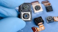
It seems that every year, one of the biggest improvements to smartphones is a newer, more technologically-advanced camera. Clearly, people care about improving photo quality. This is why the research and industry advances in the field of quantum imaging is so robust.

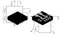
Electronic image sensing circuit. Image used courtesy of Premium Beat
Just this week, quantum image sensing company SeeDevice announced the licensing availability of their newest Photo Assisted Tunneling—Photo Detector (PAT-PD). The news allows licensing partners to integrate PAT-PD's quantum image sensing technology into their devices.
Quantum Image Sensing: How It’s Different
Before we can dive into the specifics of PAT-PD, it’s first useful to discuss the background of quantum image sensing versus traditional image sensing.
Traditional CMOS image sensors work by using photodiodes in conjunction with phototransistors to convert incident light into electrical signals. These signals are then amplified and converted into pixels via software. One of the greatest drawbacks of CMOS image sensing is that silicon isn’t terribly light sensitive.
In fact, combined with the wiring to transfer the electrical signals, each silicon sensor loses up to 75% of all light that they come into contact with.

Quantum image (left) vs DLSR image (right) in a dark room. Images (modified) used courtesy of SeeDevice
Quantum image sensing, on the other hand, leverages quantum tunneling to create a photon-activated current flow triggered by significantly fewer photons than normally required in a photo-diode-based design.
This increased efficiency is the result of layers of “quantum dots” placed on top of a conductive material like silicon. These dots are used in place of running wires to each individual photosite-like CMOS sensor. The sensor is then coated with a super black material to ensure maximum light absorption—again improving the reflective modern sensor.
Benefits of Quantum Image Sensing
Quantum image sensing technology comes with a wide range of benefits. For starters, compared to CMOS imaging, which loses 75% of incident light, quantum imaging retains up to 95% of its light. Because of this extremely high light efficiency, quantum image sensors have relatively low pixel counts, compared to CMOS sensors. The leading quantum sensors have 100,000 quantum dot photosites compared to the 2 million of regular HD.
![]()
SeeDevice claims that designers can easily integrate quantum pixel technology for any standard CMOS fabrication. Image used courtesy of SeeDevice
Requiring significantly fewer photosites for the same high-quality image gives quantum imaging sensors the added benefit of shrink-ability. Designers no longer have to trade off camera size and image quality. This technology allows for devices like smartphones to benefit from high-quality imaging.
SeeDevice's PAT-PD
SeeDevice’s PAT-PD boasts some impressive specs, especially when compared to standard CMOS sensors. One important spec in image sensing is sensitivity, normally measured in uV per electron or A/W. A standard CMOS image sensor comes in at about .15-.25 A/W in sensitivity. PAT-PD technology blows this number out of the water, claiming a sensitivity of 108 A/W.

PAT-PD responsivity vs. wavelength compared to other technologies. Image used courtesy of SeeDevice
This huge increase in sensitivity allows PAT-PD devices to sense into the 300nm–1,600nm near-infrared spectrum with plans soon to expand this range to 2,000nm. This is done while maintaining an SNR of over 60dB, ensuring high-quality images.
The device sensitivity also allows sensors to maintain high-fidelity visuals, even in extremely low-lighting conditions. Quantum tunneling technology has the added benefit of decreasing reaction time from microseconds to sub-nanoseconds while boosting dynamic range to 100dB linear and 150dB non-linear.
The Future of Quantum Image Sensing
With such a wide variety of benefits, quantum imaging seems like a promising up-and-comer in the future of image sensing. Now with PAT-PD licensing available, we may see quantum imaging making its way into more and more devices. It's possible, too, that this technology may one day appear in smartphones.