Facebook
 Google
 GitHub
 Linkedin
New Reference Designs Aim to Speed Time to Market for Mobile Chargers
Three new reference designs on the market can help designers working with USB PD, fast chargers, and in-vehicle wireless charging.
Reference designs are technical reports that help engineers and original equipment manufacturers (OEMs) avoid design risk and save on expenses; they include reports containing PCB layouts, schematics, power supply design specifications, transformer documentation, and bill of materials. Reference designs may also include comprehensive circuit descriptions, general performance data, design capabilities, thermal performance, magnetics specifications, and fast transient and electrostatic discharge (ESD) protection data.

A populated circuit board based on DER-937 reference design. Image used courtesy of Power Integrations
These documents help engineers incorporate particular solutions into specific applications. A number of companies recently released mobile charging-based reference designs to help miniaturize chargers and maximize switching efficiency. In this article, we'll review some of the specs and design benefits of these recent publications to assess how they may be of use to embedded designers.
Power Integrations Cuts Down the Component Count in USB PD
Power Integrations recently published a reference design for its InnoSwitch3-PD switcher and HiperPFS-4 controller IC-based DER-937. This technical report contains essential information on the efficient design of a USB power delivery (PD) programmable power supply (PPS) charger.
The company, a manufacturer of high-voltage power conversion-intensive semiconductors, claims the DER-937 design exceeds 93% efficiency when properly implemented. Moreover, Power Integrations says this design offers exceptional no-load performance at a minimized circuit power requirement of 40 mW at 230 VAC.
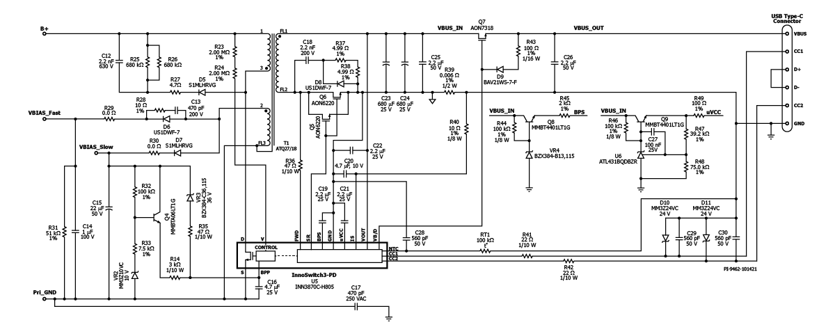
Schematic of the DER-937 reference design. Image used courtesy of Power Integrations
The DER-937 schematic above incorporates several components, including Power Integrations’ InnoSwitch3-PD switcher IC and a USB power delivery controller. The controller is essential for synchronous rectification by offering output voltage, current sensing, and gate driving capabilities.
Some key specifications of the DER-937 reference design include:
- Output voltage (VOUT) range: 3.3 V to 21 V
- Input voltage range: 90 V to 295 V
- Minimum efficiency: 92.64%
- RoHS and EU ErP compliance
- Single output
- 100 mW output power
With a low component count of 117, the reference design may provide several benefits for ultra-compact USB charger manufacturing: it is said to optimize space, shorter design times, and simplify component sourcing.
Silanna Semiconductor Accelerates Fast-charging Design
Another recent reference design comes from Silanna Semiconductor for its RD-29—an Active Clamp Flyback (ACF). Silanna says this design can help designers quickly create 65 W 1 C fast-charger applications.
The design incorporates the SZ1131 ACF controller, a new addition to its CO2 Smart Power IC family. The design also includes Transphorm’s Super GaN FET. This travel adapter and battery charger-based reference design is said to offer a few other important specs:
- Efficiency: 94.5%
- Minimized no-load power consumption: 23 mW at 230 VAC
- Footprint: 34.5 mm x 34 mm x 30.5 mm
- Power density: 30W/inch3
Silanna says the design will help engineers exceed radiated electromagnetic interference (EMI) requirements by over 6dB—a boon for developing miniaturized 65 W low power consumption chargers.

RD-29 reference design. Image used courtesy of Silanna Semiconductor
The reference design features multi-mode operation (e.g., valley mode switching, burst mode, and quasi-resonant), a high switching frequency of 140 kHz, and cycle-by-cycle adaptive digital control. Additionally, the RD-29 reference design also considers protection against overvoltage, under-voltage lockout, overvoltage lockout, overpower, and short circuit.
NXP Steps on the Gas for Automotive Wireless Charging
Lastly, NXP aims to meet the growing demand for in-vehicle wireless mobile charging with its recently-released reference design. NXP says this design is the first in the industry to be certified by the Wireless Power Consortium (WPC).
It includes a Qi-certified board with NXP wireless charging microcontrollers (MCUs), optional near-field communication (NFC), secure element, and controller area network (CAN)/local interconnect network (LIN) transceiver.
Since the reference design gives engineers access to NXP’s comprehensive wireless charging software library, they can modify a design for targeted wireless charging applications.

NXP WCT-15WAUTO13 reference design block diagram. Image used courtesy of NXP
A few other relevant features include:
- Wireless power efficiency: 75%
- Operating frequency: 127.7 kHz
- Foreign object detection functionality
- Bluetooth and Wi-Fi connectivity
- Temperature sensing capability
- Ambient operating temperature range: -40°C to +105°C
- NFC card detection
- Minimized bill of material for on-chip demodulation
- AEC-Q100 grade 2-certified
The NXP WCT-15WAUTO13 reference design is said to leverage EMC optimization and safety features. The design includes auto-grade components and automotive functions to meet each modified charging requirement. It also offers a maximum power delivery of 40 W.
Reference Designs Continue to Speed Up Development
Reference designs are essential for prototyping and integrating solutions. They save time and costs while mitigating risk. This is because reference design developers—predominantly technology component vendors—have already implemented and tested the designs. Vendors also develop and release reference designs based on their products to give them a competitive advantage.
The three recently-released designs from Power Integrations, Silanna Semiconductor, and NXP showcase how these documents can speed up the development process for both simple and complex charging applications—whether they be tailored for fast-charging or in-vehicle wireless charging.
Related Content