Facebook
 Google
 GitHub
 Linkedin
NXP Launches MCUs Blending 10BASE-T1S Ethernet and Post-Quantum Security
The new MCX A5 MCUs integrate 10BASE-T1S Ethernet, topology discovery, and post-quantum security to streamline and protect industrial edge networks.
Last week, NXP Semiconductors announced the release of the MCX A5 family, a new line of devices engineered to simplify secure connectivity for industrial and IoT edge applications. By combining high-performance processing, integrated single-pair Ethernet capabilities, and advanced cryptographic security, the MCX A5 aims to modernize industrial networks and unlock the real-time operational data required for intelligent automation.
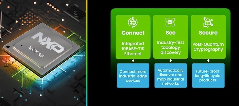
The MCX A5 MCUs feature single-pair Ethernet connectivity, advanced cryptographic security, and topology discovery.
The new microcontrollers are designed to replace isolated endpoints and legacy communication interfaces, such as RS-232 and RS-485, with modern, scalable Ethernet networking that extends directly to the edge of the factory floor.
Core Processing and Memory Architecture
At the heart of the MCX A5 is an Arm Cortex-M33 core operating at up to 240 MHz, delivering 988.8 CoreMark performance. The core features a floating-point unit (FPU), digital signal processing (DSP) capabilities, a memory protection unit (MPU), and Arm TrustZone technology. To further optimize system performance, the MCU includes a SmartDMA co-processor designed to offload peripheral and data movement tasks from the main CPU.
The devices offer substantial on-chip memory to support complex edge applications, featuring up to 2 MB of dual-bank flash with error correction code (ECC) and read-while-write support. Additionally, the MCUs incorporate up to 640 kB of SRAM, which is configurable as up to 64 kB of RAM with ECC, along with a 16 kB cache engine.
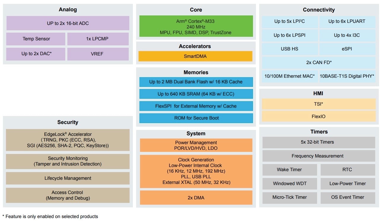
MCX A5 MCU block diagram. (Click on image to enlarge)
Despite the high performance, the MCX A5 maintains a highly efficient power profile. The MCU operates on a 1.71 V to 3.6 V supply and achieves active current consumption as low as 136 µA/MHz, alongside a deep power-down current of just 700 nA. More information can be found in the MCX A5 fact sheet.
Integrated 10BASE-T1S and Topology Discovery
A defining feature of the MCX A5 family is its approach to industrial networking. The MCUs integrate a 10/100M Ethernet MAC and a 10BASE-T1S digital physical layer (PHY). This integration significantly reduces bill-of-materials (BOM) costs and board complexity by eliminating the need for an external digital PHY.
To implement a complete IEEE 802.3cg-compliant Single Pair Ethernet (SPE) solution, developers only need to pair the MCU with an external physical medium dependent (PMD) transceiver, such as NXP’s TJF1410.
Meanwhile, the MCX A5 introduces what NXP is calling an industry-first topology discovery capability for a wired MCU. As industrial networks scale, mapping connected devices can become a complex manual process.
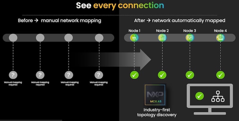
With its topology discovery capability, the MCX A5 automatically identifies and maps network endpoints.
The MCX A5 automatically identifies and maps connected endpoints, providing operators with immediate visibility into the network layout. This accelerates network commissioning, simplifies maintenance, and allows for easier expansion over time.
Future-Proofing with Post-Quantum Cryptography
Because industrial equipment often features product lifecycles extending over a decade, future-proofing network security is a critical design requirement. To address evolving cybersecurity threats, the MCX A5 incorporates a hybrid post-quantum cryptography (PQC) hardware root of trust.
Leveraging NXP's EdgeLock security technology, the hardware cryptographic accelerator supports modern standards like ECC, RSA, AES-256, and SHA-2, alongside PQC algorithms. The architecture facilitates secure boot, secure firmware updates, device attestation, and lifecycle management. NXP has designed the MCX A5 with a security architecture targeting both PSA Certified Level 3 and SESIP Level 3 certifications.
Rich Analog and Serial Peripherals
Beyond networking and security, the MCX A5 is equipped with a comprehensive suite of analog and digital peripherals tailored for motor control and embedded industrial applications.
Key peripheral features include:
- Analog Integration: Up to two 16-bit analog-to-digital converters (ADCs), up to two 12-bit digital-to-analog converters (DACs), analog comparators, a voltage reference, and an integrated temperature sensor.
- Serial Interfaces: Up to six LPUARTs, five LPI2C interfaces, six LPSPI interfaces, and four I3C interfaces.
- Advanced Connectivity: Up to two CAN FD controllers, a High-Speed USB host/device controller with an on-chip HS PHY, and a FlexSPI interface for external memory expansion.
- Timing Resources: Five 32-bit timers, a low-power timer, windowed watchdog timers, and specialized PWM event timing resources.
Ecosystem and Availability
The MCX A5 family is supported by NXP’s broader MCUXpresso unified developer experience, which includes the MCUXpresso SDK, VS Code integration, and support for both Zephyr and Rust. The hardware is backed by NXP's 15-year Product Longevity program, ensuring long-term availability for industrial original equipment manufacturers.
Target applications for the MCX A5 encompass a wide range of distributed edge nodes, including programmable logic controllers (PLCs), industrial human-machine interfaces (HMIs), factory and building automation systems, energy management controllers, and smart data center infrastructure. The MCUs are available in multiple package options, including WFBGA169, LQFP144, and LQFP100.
All images used courtesy of NXP.