Facebook
 Google
 GitHub
 Linkedin
Researchers Get Creative With Fab Techniques for Semiconductor Advances
From thermal annealing to atomic-level lift-off, researchers are rethinking fabrication bottlenecks to unlock new performance ceilings in semiconductors.
Teams from the University of Michigan, MIT, UW–Madison, and PolyU have recently demonstrated how novel process tweaks, not just new materials, can yield significant gains in device performance and scalability. These manufacturing techniques can advance applications spanning piezoelectric sensing, infrared imaging, and solar energy.
Thermal Tweaks Supercharge Piezoelectric Films
At the University of Michigan, engineers have achieved an eightfold boost in the piezoelectric response of scandium aluminum nitride (ScAlN)—a material already viewed as a successor to legacy ceramics like PZT. The twist? A simple post-growth thermal annealing step that heats the material to 700°C for two hours, realigning misoriented crystal grains and dramatically improving electromechanical performance.
Piezoelectric materials convert pressure into electrical signals and vice versa, playing critical roles in RF filters, ultrasound probes, vibration sensors, and energy harvesters. But in nitride-based films like ScAlN, the full performance potential has long been limited by microscopic imperfections introduced during deposition.
_and_doctoral_student_Shubham_Mondal_(right).jpg)
Professor Zetian Mi (left) and doctoral student Shubham Mondal (right) discuss their research. Image used courtesy of Marcin Szczepanski, University of Michigan
By correcting these defects and enabling uniform grain orientation, the Michigan team increased the piezoelectric coefficient (d₃₃) from 12.3 pC/N to 45.5 pC/N—well beyond the 6–7 pC/N typical for aluminum nitride in current 5G devices. Importantly, the enhancement doesn't require new tooling or exotic fabrication techniques, making it highly compatible with existing semiconductor workflows.
Applications range widely: higher-sensitivity microphones, medical ultrasound with better image clarity at lower power, traffic-powered sensors embedded in smart roads, and low-power IoT nodes that harvest ambient mechanical energy. DARPA is already backing the research for use in atomic clocks, hinting at serious interest from the defense sector.
This annealing technique could become a standard add-on step in MEMS and RF front-end production, offering a low-cost route to high-performance piezoelectric components.
Atomic Peel-Off Yields Ultra-Thin “Skin” for Infrared Vision
MIT and the University of Wisconsin-Madison have cracked a long-standing barrier in electronic materials fabrication: how to mass-produce ultrathin sensing films without sacrificing performance or scalability. The result is a 10-nanometer-thick pyroelectric membrane, currently the thinnest ever fabricated, that can detect subtle thermal changes across the entire infrared spectrum—no cooling required.
Unlike traditional far-IR sensors that rely on bulky cryogenic systems, the new membrane operates at room temperature, offering performance on par with state-of-the-art night-vision technology. That alone positions it as a game-changer for next-gen night-vision eyewear and autonomous driving systems, where weight, power, and footprint are critical.
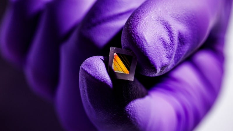
The new film could give rise to lighter, more portable, and highly precise far-infrared sensing devices. Image used courtesy of Adam Glanzman, Massachusetts Institute of Technology
The key innovation is a novel atomic lift-off (ALO) technique. Using a pyroelectric material called PMN-PT, researchers found they could cleanly peel the ultrathin film from its substrate without a release layer thanks to lead atoms acting like atomic-scale Teflon. These atoms prevent bonding during growth, enabling defect-free separation and transfer to flexible electronics or chip-scale arrays.
With a record-high pyroelectric coefficient and exceptional thermal sensitivity, the freestanding films open new frontiers for wearable sensors, IR cameras, smart textiles, and thermal diagnostics in electronics. Better yet, the ALO method is generalizable; other materials can be tuned for similar peel-off behavior, making this not just a one-off lab success but a viable platform for scalable thin-film manufacturing.
As the team moves toward system integration and environmental testing, the path from cleanroom to commercial reality is already forming, bringing lightweight, power-free IR sensing to everything from night-vision glasses to self-driving cars.
PolyU Cracks the Efficiency Ceiling With Record-Breaking Tandem Solar Cells
At the Hong Kong Polytechnic University (PolyU), researchers have achieved what many in the solar industry have long chased: a certified 33.89% power conversion efficiency (PCE) in perovskite/silicon tandem solar cells, officially surpassing the Shockley-Queisser limit for single-junction devices. More than a record, the milestone demonstrates a viable path to commercially scalable solar technologies that break through long-standing theoretical barriers.
The key innovation was a bilayer interface passivation strategy, addressing one of the most persistent obstacles in tandem solar development: charge loss due to interfacial recombination between the perovskite layer and the electron transport material. The PolyU team layered an ultrathin lithium fluoride (LiF) film with short-chain ethylenediammonium diiodide (EDAI), achieving synergistic field-effect and chemical passivation. This technique significantly boosts carrier lifetime and suppresses nonradiative recombination, one of the major efficiency bottlenecks in tandem cell architectures.

Professor Yin Jun, assistant professor of the Department of Applied Physics at PolyU, pioneered the novel bilayer interface passivation strategy to develop efficient tandem solar cells. Image used courtesy of PolyU
From a fabrication standpoint, PolyU also implemented a double-textured silicon heterojunction base that maximizes light trapping while preserving high rear-side passivation. The result was not only a PCE of 33.89%, but an 83% fill factor and open-circuit voltage nearing 1.97 V—all while demonstrating strong operational stability.
This process works across multiple perovskite chemistries and is compatible with both vacuum and solution-processed deposition methods, giving it real industrial potential. Applications include high-yield rooftop panels, next-gen solar farms, and even integrated power solutions for IoT and edge systems where power density is critical.
With industrial collaborators like Longi and growing competition from Jinkosolar and Trinasolar, PolyU’s bilayer strategy may well define the next phase of high-efficiency photovoltaics, moving perovskite tandem cells from R&D into robust, market-ready platforms.
Related Content