Facebook
 Google
 GitHub
 Linkedin
Rohm Unveils Tiny MOSFET Aimed at Fast Charging Applications
The new power MOSFET offers low ON-resistances combined with a compact 2.0 mm × 2.0 mm package.
Rohm has developed an ultra-compact MOSFET featuring an industry-leading low ON-resistance directed at improving protection and simplifying circuit integration.
The AW2K21 power MOSFET optimizes fast charging functionality for compact devices, such as smartphones, in a small mold package.
The need for fast charging functionality in large-capacity battery devices leads smartphone manufacturers to demand strict specifications for MOSFETs, due to the high current transfer involved.
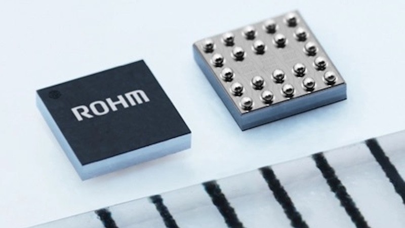
AW2K21 power MOSFET
Challenges to Shorten Charging Times
Fast charging functionality requires bidirectional protection to prevent reverse current flow to peripheral ICs and other components when not actively supplying or receiving power. In addition, it generates high current power transfer, which requires MOSFETs to have advanced features, including a maximum current rating of 20 A, breakdown voltage between 28 V and 30 V, and an ON-resistance of 5 mΩ or less.
Unfortunately, standard solutions result in increased board space and mounting complexity, as they require the use of two large, low-on-resistance MOSFETs.
AW2K21 Power MOSFET
In response, Rohm designed the AW2K21 where two MOSFETs are integrated into a single package, allowing a single part to support bidirectional protection applications (commonly required in power supply and charging circuits).
This newly developed 30 V, 20 A N-channel power MOSFET comes in a common-source configuration that achieves an industry-leading on-resistance of 2.0 mΩ (typical) in a compact 2.0 mm × 2.0 mm package.
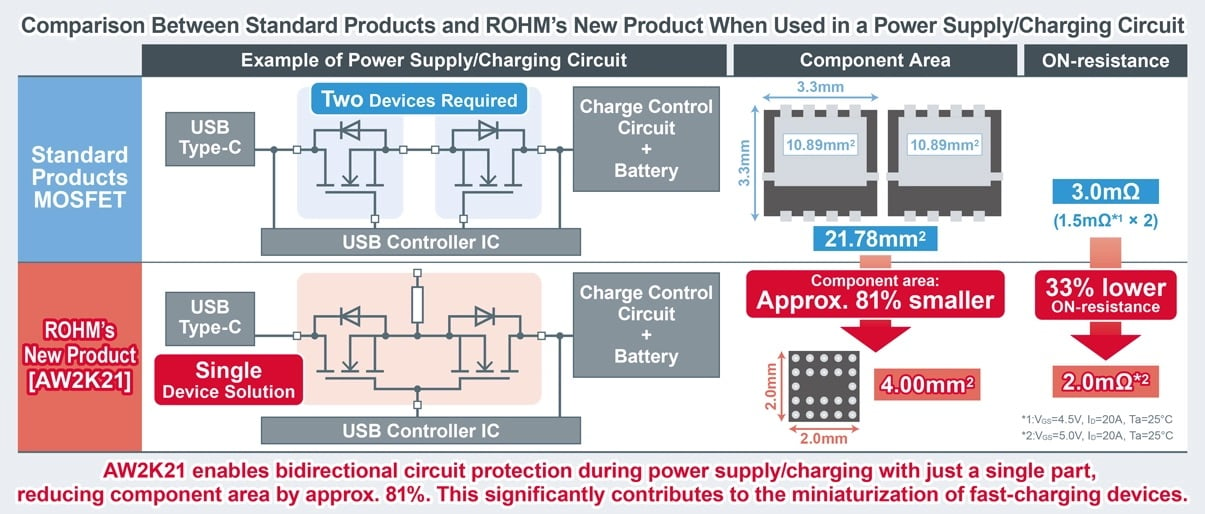
Comparison between standard products and Rohm’s new products. (Click on image to enlarge)
Key Role of ON-resistance
The AW2K21 adopts a proprietary structure that enhances cell density while minimizing the ON-resistance per unit chip area. The use of a WLCSP is enabled by placing the drain terminal on the top surface, unlike on the backside in standard vertical trench MOS structures.
This makes the new product ideal for high-power fast charging applications, minimizing power loss and enabling high-current operation despite its ultra-compact size. More information can be found in the AW2K21 data sheet.
The Value of its Tiny Footprint
This size reduction is most apparent in power and charging circuits for compact devices, where standard solutions typically require two 3.3 mm × 3.3 mm MOSFETs, while the AW2K21 can achieve the same functionality with a single 2.0 mm × 2.0 mm unit, reducing the footprint and consequently ON-resistance by approximately 81% and 33%, respectively
This contributes to lower power consumption (only 1.6 W) and increased space savings across a variety of applications. It’s suitable for USB VBUS Protection, Battery Protection, and Load Switch.
Suitable Applications and Use Example
The most convenient apps are those equipped with fast charging capabilities, including smartphones, tablets, laptops, wearables and drones, among others.
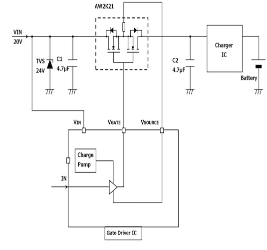
Usage example: USB PD Circuit
The AW2K21 data sheet offers these recommendations for using the device in a circuit:
- It is recommended to connect a capacitor of 4.7 uF or more as close as possible to both input and output of this product.
- It is needed to connect a TVS (Transient Voltage Suppressor) as a protective element against surges that exceed the absolute maximum rated voltage.
- This product might cause chip aging and breakdown under the large electrified environment. Please consider designing an ESD protection circuit.
Pushing the Limits
Clearly the new AW2K21 addresses demands for compact, high-power fast charging solutions, leveraging the device’s integrated bidirectional protection and good ON-resistance. This device is likely to enable more compact and sustainable electronic systems across diverse applications, paving the way for future innovations in power management.
All Images used courtesy of Rohm.