Facebook
 Google
 GitHub
 Linkedin
Siemens Cuts Down IC Development Time With New EDA Tool
At DAC this week, Siemens is rolling out an IC design tool suite that it claims enables “correct-by-construction” design changes earlier in the cycle.
The 60th annual Design Automation Conference (DAC) kicks off this week in San Francisco. The industry's premier EDA tradeshow is already running from July 9-13 at San Francisco's Moscone West venue.
Like every year, Integrated circuit (IC) design is a leading topic at the show. IC design is a notoriously slow process, requiring many intricate steps and iterations to get right. To make matters more complicated, the extremely high cost of tapeout shrinks the margin for error in the design process. Because of this, powerful and feature-rich EDA tools can have a significant impact on the success and time to market of new chips.

The standard IC design process vs. the shift-left approach
Feeding those needs, today at DAC, Siemens Digital Industries Software (formerly Siemens EDA) announced the launch of Calibre DesignEnhancer, a new EDA tool developed to enable faster tapeout while improving design manufacturability and circuit reliability. In this piece, we’ll take a look at three of the major features of Calibre DesignEnhancer to explore how this platform might aid IC designers.
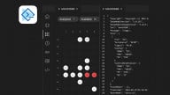
Via Optimization
The via modification feature is one of the three major use models from Calibre DesignEnhancer. Dubbed DE Via, this feature is designed to enhance the yield and reliability of IC designs by automatically adding design rule checking (DRC) clean vias to the design.

DesignEnhancer via optimization tool
The tool can automatically analyze layouts and insert over a million "correct-by-construction" vias. To do this, the tool uses manufacturing requirements provided by the foundry to determine the requirements for via insertion. These requirements are then used as input to the ASCII-based Calibre DesignEnhancer Via kit, which can be modified by IC designers or process design kit (PDK) developers as needed.
Additionally, the tool is equipped with a push-button via modification feature that optimizes available design space (including multi-layer operations), ensuring the maximum via insertion rate. With these features, DE Via may help designers meet their power goals without impacting performance or area metrics.
Filler Cell Insertion
The next of the three use models from Calibre DesignEnhancer is the filler cell insertion tool.
Called the Physical Verification-Ready (Pvr) model, the filler cell insertion tool aims to cut down on the time to reach a DRC-ready design by automatically inserting cells. Specifically, the tool inserts correct-by-construction filler cells, decoupling capacitor (DCAP) cells, and engineering change order (ECO) filler cells into IC layouts post-design implementation.

Calibre DesignEnhancer Pvr significantly enhances design time.
According to Siemens, the Pvr model uses DCAP insertion to enhance the quality of results and meet designers' density specifications. Over the span of a design flow, the tools’ correct-by-construction approach is said to significantly reduce overall runtime, allowing designers to achieve tapeout quicker.
Power Grid Enhancer
The final feature of Calibre DesignEnhancer we'll cover is the Power Grid Enhancer (Pge) model.
Designed to optimize power and ground structures in IC layouts, DE Pge performs an automatic analysis of layouts and inserts DRC-clean vias and interconnects in open tracks. This process creates parallel runs, effectively lowering resistance and mitigating issues related to internal resistance and electromigration within an IC's power delivery network.

IR drop improvements with DE Pge
The model is uniquely capable of focusing layout enhancements in specific areas. This targeted approach can reduce IR drop while minimizing any potential impact on timing. Siemens claims the tool not only enhances the power and ground structures but also maintains the overall performance of the IC layout.
The company reports that users of Pge have reported substantial improvements, with IR drop issues reduced by up to 90% in some cases.
Making IC Design Easier
While IC design has gained a reputation for being difficult and time-consuming, it doesn’t necessarily have to be that way. With its new DesignEnhancer tool, Siemens is introducing a number of important features to the IC design workflow, aiming to create better designs in faster times. With the ultimate goal of pushing more reliable designs to tapeout faster, Siemens’ new DesignEnhancer may be a strong choice in the IC EDA market.
According to Siemens EDA, Calibre DesignEnhancer kits are noew available for all leading foundries supporting designs from 130 nm to 2 nm, depending on the use model and the technology.
More information is available in the Calibre DesignEnhancer fact sheet.
All images used courtesy of Siemens