 Facebook
 Google
 GitHub
 Linkedin
Teardown Tuesday: Mini Network Router
In this teardown, we will look inside a mini router that creates a wireless local area network.
Devices connecting to the internet are increasingly using wireless connections as opposed to a wired connection. Such a connection reduces clutter and cost while barely sacrificing on data transfer speeds. In this teardown, we will look inside a mini router that creates a wireless local area network.
Key Parts
The Casing
The router sits in a small moulded plastic container which has various IO ports and LED indicators. The sides of the router include a small vent, ethernet ports, USB power ports, and buttons. The top side of the case has three indicators which indicate power, user configuration, and wireless network enablement.

The wireless mini router

The vent on the side

Various IO and a second vent

Ethernet ports on the other side
The underside of the case includes all the product information including the unit's IP address, model number, SSID, default password, and MAC.

Underside showing information and more vents
The casing is made up of two parts: the top square container and a base that is held in using wedge-shaped clips. Opening the unit only requires a small flat head screwdriver and a bit of prying, popping the base off the unit.
The PCB inside the unit is not held in with screws or fittings but instead sits in plastic pieces that fit into holes on the PCB.

The view once the base comes off

The PCB removed
The PCB: Underside
The underside of the PCB reveals some interesting PCB production techniques as well as a mixture of surface-mount and through-hole parts.
The ethernet connectors show resistors and capacitors connecting to IO which are typically used to smooth edges on switching signals. Smoothing is needed because signals which have sharp edges produce harmonics which can interfere with nearby electronics. Such interference would break FCC and CE regulations, so a product must comply with those regulations to be eligible for sale.

Ethernet and passive components for smoothing
Near the USB A connector is an 8-pin IC surrounded by various passive components. This part, identified as AZ88 (or possibly AZ8B), does not have a datasheet that can be found online. However, considering that this unit is provided power over the USB connector, as well as the use of large capacitors and an inductor, it is fair to say that this could be a DC-DC converter that produces a 3.3V source from the 5V USB. Another tell-tale clue is the size of the traces connecting to the various pins.

"AZ88", most likely a DC-DC converter
Just below is a Winbond 25Q128FVSG which is a 3V 128M-Bit (16MB) serial flash memory IC in an SOIC package. This most likely contains boot information for the main controller as well as storing information such as SSID, network configuration, and other important parameters.

The 25Q128FVSG
Just below the memory IC is a portion of missing power/ground plane. This has been done because the opposite side of the board has a PCB antenna. The ground plane, which is fantastic at absorbing stray EM signals, would severely inhibit the device's ability to send and receive signals.

The missing plane for the Wi-Fi antenna
The underside also contains many resistors connected to traces as if they were series resistors in a bus of some kind. The other side of the PCB contains a few large ICs that are obviously to do with data processing and so it would make sense if these resistors are series resistors. Series resistors on fast-changing signal traces perform two functions:
- limit current and help to prevent damage to parts
- help to prevent reflections
While current limiting is unlikely, reflections can be a serious problem in high-speed circuitry. When a signal is sent down a PCB trace, impedance mismatches between the source and destination can result in electrical signals “bouncing” back and forth. This is an issue because it can confuse devices into thinking that there is a valid signal on the line. Series resistors not only help to match the impedances but also help to resist against these reflections.

Series resistors on a bus

Some more series resistors
The last two parts of interest on the underside are the 25 MHz crystal and some gold lines. These gold lines are connected to the floodplain and their function is not known. If you can shed light on this, let me know in the comments below.

Crystal and gold line
The PCB: Topside
The topside of the PCB contains through-hole and surface-mount components, as well as the main ICs that make the product.

The main PCB
The first IC of interest is the large Atheros SoC which is identified as an AR9331-AL3A. This SoC is specifically designed for use with 2.4GHz 802.11n communication and includes a MIPS 24K core, five ethernet switching ports, USB, I2S, UART, and GPIO. This processor uses JTAG debugging, which means that somewhere on this PCB we may find a debugging port or header that could allow this product to be reversed engineered.

Main processor, the Atheros AR9331-AL3A
Next to the SoC is the elixir N2DS51216DS, which is a 512Mb SDRAM high-speed CMOS memory IC. This IC would explain the large number of series resistors found underneath the PCB (these resistors would sit in the middle of the address and data lines).

The memory SDRAM IC, elixir N2DS51216DS
Next to the SoC is the Wi-Fi antenna on the PCB and, interestingly, the antenna trace also has an antenna port connected to it. This may have been put in during development for debugging reasons but why it's included on the PCB now (considering the lack of an external antenna) is beyond me.
Next to the antenna port (labeled as J13) is a fiducial used for pick-and-place machines, various surface-mount parts, and a surface-mount switch.
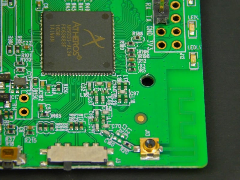
Antenna, ports, and components

More IO and components
Interestingly, the product contains a three-pin header which is clearly connected to a UART port (Rx and Tx give that away). The function of this is most likely to either bootload code into the main SoC and/or upload data into the serial flash.
Since it is unlikely that the company that produces this product gets memory pre-programed, they will program the devices themselves once the unit has been constructed. The pin header allows an employee to connect up a header and click “download” on the PC, which flashes the device.

The program header
Summary
This network router demonstrates not only how SoCs are taking over but also how PCB layout and design is still critical in modern products. Just because many parts are being integrated into a single package does not mean that key PCB techniques such as the use of ground planes, stitching vias, series resistors, and plenty of EMC control are unneeded.
Next Teardown: Bluetooth Sony Speaker
Related Content


The gold strips are interesting to me as well, my first thought was that it could be used for some kind of shielding to connect to the ground plane, but there is no shielding. By the way, the UART and un-populated GPIO connectors are meant so someone can “hack” the router. It is marketed on Amazon as such. Also note that the “vents” on the side are meant for external antennas that you can buy separately on installed on other models. See - https://www.amazon.com/GL-AR150-Openwrt-pre-installed-Repeater-Tethering/dp/B015CYDVG8/ref=sr_1_11?ie=UTF8&qid=1495763380&sr=8-11&keywords=diy+router
The gold strips are on the underside of the PCB which would make the side that could be wave soldered. You can see the through hole legs poking through the PCB close by. The top would be reflow soldered in an oven say. From the PCB design stage if this was viewed as going through a wave solder oven, then the strips are to improve current carrying on a ground plane. This may not be necessary once the product is finalized, but saves a step in the design and testing process if possible.
Wade
So it was not used and they remain as gold visible strips.
The gold strips likely help with heat dissipation. This would make sense as they are located below the soc.