 Facebook
 Google
 GitHub
 Linkedin
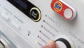
Teardown Tuesday: Google Home Mini
In this teardown, we inspect the guts of Google’s voice-activated home assistant, the Google Home Mini.
In this teardown, we inspect the guts of Google’s voice-activated home assistant, the Google Home Mini.
First Impressions
Being a newbie to voice-activated home assistant devices, I wasn’t quite sure what to expect during the unboxing of the Google Home Mini. I must admit that after removing the chalk-colored voice assistant from its packaging, I said out loud: “This is it?” That's how small it is—it measures only 3.85” in diameter and 1.65” in height.
Nonetheless, it did feel like a solidly-built piece of technology: no loose speaker cover, no flimsy plastic pieces, and no metal/plastic pieces rolling around on the inside as I completed my visual inspection.
The first step of the disassembly process was to locate the hidden screws that held the unit together.

Google Home Mini
A Hunt for the Screws
After prying, pulling, and twisting the device with the hopes of locating those darn screws, I realized they must be hidden under the brightly-colored rubber-like base plate covering. Removing this rubberized cover was not trivial—at least, not until it met my heat gun.
After warming up the rubber cover a bit (actually, I had to get it quite hot), I was able to peel it off. If you’re worried about this rubber cover coming off with years of use and abuse, don't. It’s not going anywhere.

A heat gun was required for removing the rubber base plate covering.
Removing the Screws and Viewing the Components
Once the rubber base plate covering was removed, four Torx screws were exposed.

Four Torx screws reside under the rubber base plate covering.
After removing these four screws and then subsequently removing the white plastic cover, four more screws were observed holding the speaker housing in place. Also in view was a simple PCB which held the USB connector and a flex circuit (used for bringing power to the internal electrical components). Using a flex circuit is a much cleaner, and perhaps more durable, design approach when compared to using simple wires or a cable.

Simple PCB and flex circuit, and the speaker housing.
With the speaker housing removed, we can see a cone-shaped metal/plastic hybrid plate and, of course, the speaker itself.

Cone shaped metal-plastic plate and the speaker.
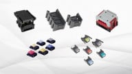
The lone speaker (see images below), which looks to be either a full-range or midrange speaker, has a fairly large magnet on it. As you can see, the speaker was contained inside its plastic-welded enclosure. Sealing the speaker enclosure in this manner increases the overall sound quality of this rather small speaker.

The speaker's cone.

The speaker’s magnet.
Metal/Plastic Hybrid Cone-Shaped Plate
The metal/plastic hybrid cone-shaped plate is designed to redirect the sound waves with the intent of increasing the sound quality of the device. The reason for having the two strategically-located black plastic pieces is that they allow for the RF signals (Wi-Fi and Bluetooth) to reach the device’s antennas.
And you might ask, “why not use plastic for the entire plate instead of using part plastic and part metal?” The answer is heat dissipation/thermal relief (see images below).

Metal/plastic plate with a sound wave redirecting cone.

Metal/plastic plate serves as a heat sink.

Metal discoloration due to heat.
The Main PCB
As can be seen in the image below, the main PCB connects to the volume up and volume down capacitive touch sensors using gold plated contacts (on the sheet metal parts) and a gold-plated PCB surface finishing.
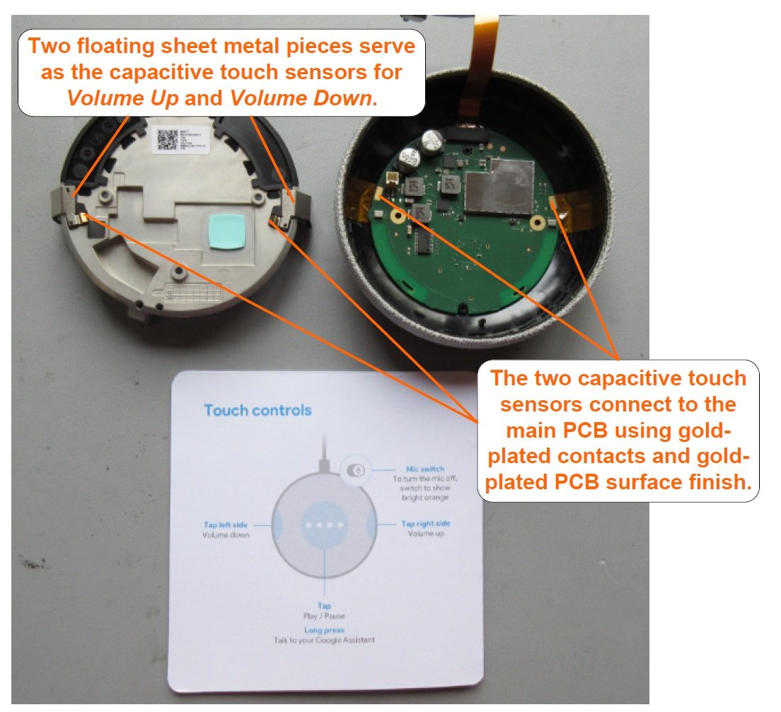
Capacitive touch controls and the main PCB.
The main PCB looks to be professionally designed and manufactured. To help keep costs down, this board is limited to a two-layer design (i.e., there are no internal layers). However, gold plating is used in some critical areas to help with long-term use and reliability, despite resulting in an increase in board cost.
The image below calls out the primary components used on this side of the PCB. Note that the main processor uses an EMI shielding box (to help reduce EMI noise) and also uses TIM (thermal interface material) to transfer its heat to the EMI shielding box, which, as we’ve already seen, uses TIM to transfer the heat to the metal plate.

Main PCB: front side and primary components.
- Main processor: Marvell 88DE3006-BTK2. Also referred to as Marvell’s ARMADA® 1500 Mini Plus.
- MEMS microphones: Part marking: S19548562. No additional information could be found.
- Memory (EEPROM): Toshiba TC58NVG1S3HBA16
- Audio amplifier: Texas Instruments TAS5720
- LED driver: NXP PCA9955BTW
The EMI metal shielding box looks to be perfectly (i.e., no gaps) soldered to the PCB (see image below). Such high-quality assembly and solder process allows the EMI shielding box to serve, as much as reasonably possible, as a Faraday cage.

The EMI shielding box is perfectly soldered to the PCB (i.e., there are no gaps) creating an ideal Faraday cage.
The back side of the PCB and its primary components can be seen in the figure below. This side uses two EMI shielding boxes, and both are perfectly soldered to the PCB. However, to gain access to the components underneath the shielding boxes, both boxes have been removed.
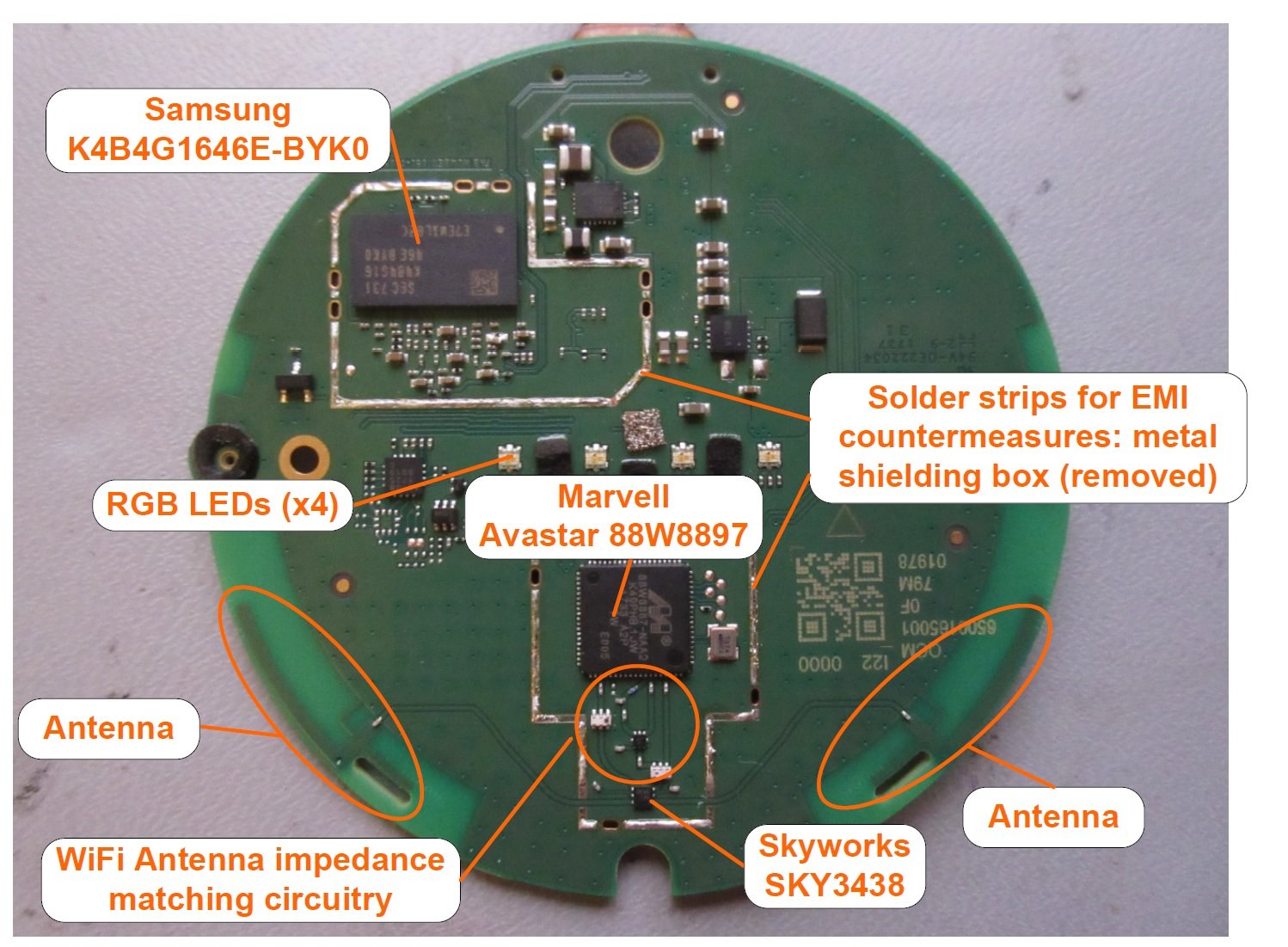
Main PCB: backside and primary components.
- Wi-Fi combination radio chip: Marvall Avastar 88W8897(PDF). Additional information can be found here.
- Memory (DRAM): Samsung K4B4G1646E-BYK0(PDF)
- Antenna switch: Skyworks SKY3438. No datasheet could be found, but it appears to be similar to this one(PDF).
Summary
By all measures, the Google Home Mini appears to be a professionally designed and expertly assembled voice-activated home assistance device. Although it is a rather small device, it definitely delivers when it comes to technology features.
Next Teardown: iPhone S6


It’s hard to tell from the photo, but the “heat stain” may be silicon oil bleeding from the TIM material. Some brands of TIM have that issue.
Very impress with article… I was able to fix my unit…with perfection…
You have done impressive deep dive, good work