 Facebook
 Google
 GitHub
 Linkedin
PCB Copper Trace Finish: Materials and Plating Methods
In this article, we discuss why PCB copper traces should be plated, and we’ll review various plating materials and plating methods.
In this article, we discuss why PCB copper traces should be plated, and we’ll review various plating materials and plating methods.
PCB Trace Plating
All traces found on external PCB layers (as opposed to internal layers) must be protected from the elements. If left unprotected, the copper will oxidize and deteriorate, making the circuit board unusable. An obvious visual sign of corroded copper is its color—it will be green. One famous example of copper oxidation is the Statue of Liberty. PCB copper plating—also known as copper coating, copper finish, and surface finish—has two essential functions: (1) to protect the exposed copper circuitry, and (2) to provide a solderable surface when assembling (soldering) components to the PCB. A variety of PCB copper plating options exist, and each carries its own advantages and disadvantages.
HASL
Hot air solder leveling (HASL), is known as the tried-and-true copper plating method. This process works by dipping a board in molten solder and then leveling it off with a hot air knife, hence its name.
HASL is known for being the least expensive type of PCB surface finish, for being widely available, and for being very economical. Other advantages of using HASL include being able to easily rework the copper finish, providing a long copper finish shelf life, and serving as an ideal option for through-hole and/or larger SMT components on your PCB. However, you might run into problems if your board uses either SOIC or small SMT components.
Some other disadvantages include having uneven surfaces, possible solder bridging, plugged or reduced plated through-holes, and, of course, HASL uses lead, so this option isn’t viable for projects requiring RoHS-compliance. If your project does indeed require RoHS-compliance, you might need to consider using lead-free HASL. Lead-free HASL is a process similar to HASL only without the lead, specifically the tin-lead solder. Materials used, in place of the lead, are tin-copper, tin-nickel, or tin-copper-nickel germanium. Although this lead-free HASL process is an economical one that offers RoHS compliance, it’s similar to the regular HASL process in the sense that it’s not ideal for smaller components.

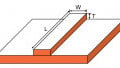
Figure 1. Example of HASL (Hot Air Solder Leveling) copper plating. Image courtesy of Sunstone.com.
Immersion Tin
Immersion coating methods utilize a chemical process for depositing a flat metal layer directly on the copper traces. Besides providing a flat surface for parts to be soldered to, tin immersion does not require the use of lead; therefore, this process yields a RoHS-compliant PCB surface. Unfortunately, the use of tin allows for the possibility of tin whiskers (see figure below).

Figure 2. Example of tin whiskers. Image courtesy of PCBheavan.com.
OSP
OSP (Organic Solderability Preservative) is a process that protects the copper surface from oxidation. According to smta.org (slide 15), “OSP is applied through chemical adsorption on the copper surface – no metal to metal displacement.” In addition to providing a lead-free flat surface, this process is advertised as being a low cost and a simple process that is very eco-friendly. Known disadvantages of using OSP include: not being the ideal choice for plated through-holes or plated-vias, having a short shelf life, and may cause issues with ICT (in-circuit testing).
ENIG
The ENIG (Electroless Nickel Immersion Gold) finish has historically been the best fine-pitch (flat) surface and lead-free option worldwide, according to multicircuits.com. ENIG is a two-step process that layers a thin coating of gold over a thin coating of nickel. The nickel serves as a barrier to the copper and is the surface to which the components are actually soldered to while the gold protects the nickel during storage. Despite the fact that this coating process yields a long shelf life and is good for plated through holes, it is a complicated and an expensive process (remember that it’s a two-step process) that is not re-workable and is known to cause signal loss in RF circuits.

Figure 3. ENIG finish. Image courtesy of internationalcircuits.com
Hard Gold
Hard gold, technically known as hard electrolytic gold, consists of a layer of gold plated over a coating of nickel. Hard gold is known for being exceptionally durable and is often used in high-wear areas such as edge connector fingers. According to bayareacircuits.com, the gold is typically 98% pure 24-carat gold with an application thickness of 30 to 50 microinches deep. However, because of its high cost and its relatively poor solderability, hard gold is not generally applied to solderable areas.
Carbon Ink
Using carbon ink in place of hard gold is an option that offers lower costs and high robustness. According to bestpcbs.com, using carbon ink reduces material costs by replacing gold with carbon, and reduces process costs by “replacing the electrolytic bath with a simple screen-printing process.” And regarding robustness, “Tests have shown that a typical carbon ink is hard enough to withstand >1 million pushbutton operations (keypad) or 100 insertion operations ... (edge connector) without showing wear or increased resistance.” However, it has been noted, again from bestpcbs.com, that “carbon inks must have good viscosity stability for warmer climates and require good printing properties to give even coverage over the copper pads.” Another disadvantage is that the cured carbon ink must be able to withstand process steps including “solvent cleaning and soldering without loss of adhesion and conductivity.”

Figure 4. Carbon ink finish. Image courtesy of bestpcbs.com
IPC Standards for Surface Plating
IPC provides standards for final finish, surface plating, and coating thickness requirements (see table below).

Figure 5. IPC standards for surface plating requirements. Image courtesy of ipc.org (click to enlarge).
In Conclusion
Bare PCB copper traces should always be coated with an anti-corrosion surface finish for protecting the exposed copper from oxidization and deterioration. Although many surface plating options are available, it’s in your best interest to research which one is most applicable for each individual design and end-use application.


I like the ENIG, but good luck finding it on anything but high-end products like medical devices.