 Facebook
 Google
 GitHub
 Linkedin
Teardown Tuesday: Walabot In-Wall Imaging Sensor by Vayyar
In this teardown, we take apart Vayyar's Walabot DIY In-Wall Imager to see what we can find.
In this teardown, we take apart Vayyar's Walabot DIY In-Wall Imager to see what we can find.
First Impressions
To be completely honest, when I first unpacked this imaging device I was rather unimpressed: the device felt light, it felt a bit cheap, and I wasn't expecting to be dazzled. But after doing some research and watching a related YouTube video about this Walabot DIY In-Wall Imager, by Vayyar, and its underlying technology, I quickly become quite intrigued. Unfortunately, I wasn't able to connect the Walabot imaging device to my phone, an iPhone, as the device is only compatible with Android phones...bummer for me! Oh well, let's start the teardown.

The packaging material in which the Walabot DIY In-Wall Imager arrived in. Nothing special here.
Unpacking the Box
The following five items were included in the box (see image below):
- The Walabot imaging sensor itself.
- A Micro-USB to Walabot cable.
- A USB Type-C to Walabot cable.
- A gel pad—used to hold the Walabot to your phone.
- Plastic film. Intended to protect your walls (from scratches) when moving/dragging the Walabot device on them.

The Walabot DIY In-Wall Imager and its accessories.

The front and back sides of the Walabot DIY In-Wall Imager.
A Simple Enclosure
While the device initially feels a bit flimsy, as I mentioned before, it does not have the markings of being a fragile or otherwise haphazardly thrown together enclosure. In fact, the enclosure looks to be a very simple and sturdy (if unassuming) design.
While four metal screws are used to hold the two enclosure pieces together, separating them still required some minor "encouragement"—a few clips integrated into the enclosure's pieces, littered on the outer edges, help keep the two pieces tightly secured together. Once the two plastic pieces are separated, the sole internal PCB simply detaches with a little force (i.e., no additional screws secure it to the enclosure).
The following image shows the inside plastic structural design—to achieve robustness, while reducing the overall weight of the device—as well as the PCB.
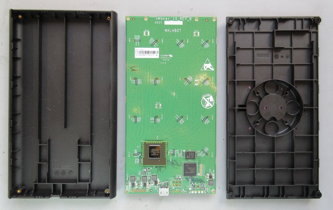
Plastic enclosure structural design and the single PCB.
The PCB
At first glance, the PCB may appear to be only moderately complex in design; besides having many passive components (capacitors and resistors) and antennas, there are only nine ICs.

The two sides of the sole PCB. At first glance, its design appears to be only moderately complex.
However, while the associated schematics of this design—which, by the way, are most likely locked away in some vault—may not be too complicated, upon further inspection of the PCB, I've come to the conclusion that the layout of the design is quite complicated. There are an obviously high-end processor and fifteen individual antennas, all of which have their transmission lines protected by Faraday cages; the transmission-line traces are buried in the internal layers of the PCB (most likely with ground planes on adjacent layers), along with stitched vias (connected to ground) on the sides of the traces.
Based on the manner in which the stitched vias have been placed—meaning their meandering routes and the close, but not identical, spacing between each of the vias, I assume all these hundreds (perhaps thousands) of vias were manually placed/routed, as opposed to being autorouted. This stitched via meandering technique can be more clearly identified in the figure below.
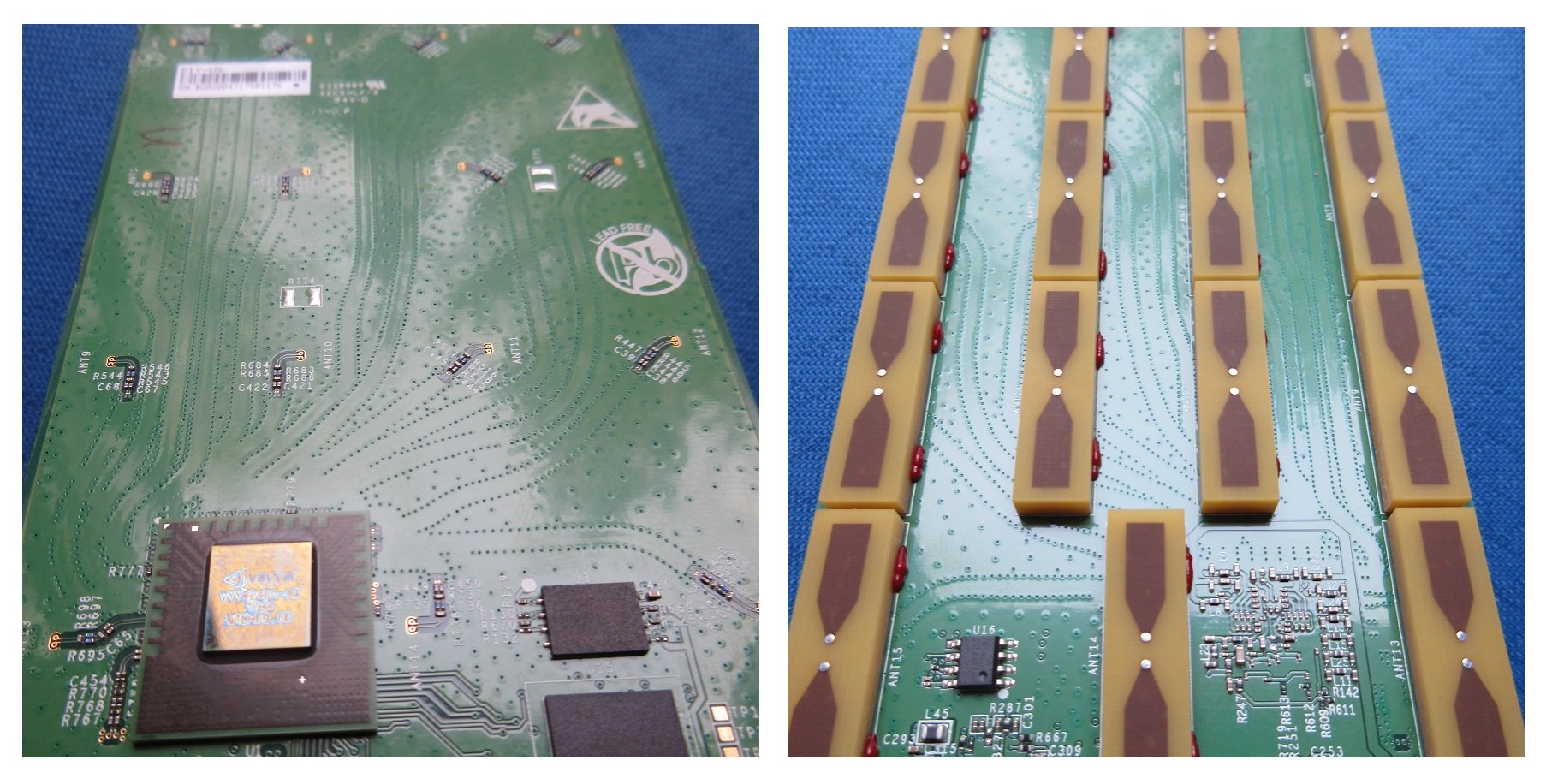
The meandering stitched vias, which serve as Faraday cages for the antenna transmission lines, appear to be painstakingly manually routed. [click to zoom]
If you have experience with routing stitched vias and think that these vias were indeed placed using an autorouter, then please let us know.
Identifying the Major Electrical Components
The primary electrical components of the design have been called out below. And while the capacitors and resistors are indeed of the utmost importance when it comes to the matching network for the transmission lines and antennas, I haven't identified these components individually. I will say, however, that nearly all of the resistors and capacitors on the PCB are 0201 parts, meaning they are super small and can be very difficult to rework/replace unless you have the right solder tools and skill set. There's a close-up image of said matching network caps and resistors below.

Components identified on the PCB's top side.
- Processor: Part marking: VYYR2401
- Serial flash memory: Part marking: 25P28V6G
- USB controller: Part marking: CYUSB2014
- Voltage regulators: Part marking: OFA (no datasheet could be found)
As can be seen in the image above, the processor is mounted on an individual PCB which is, in turn, mounted to the Walabot's PCB. When viewing the image below, it's obvious that the electrical connection between these two PCBs is achieved using a BGA.

The processor's PCB is attached to the Walabot's PCB using a BGA.
I count 36 balls on the one side, so this means that the total number of balls on this BGA approaches 1300 (36x36=1296). Impressive! Replacing this device would most definitely require a rather high-end rework solder station, and a very special skill set.
The bottom side of the PCB is where the fifteen antennas live. The following image identifies these antennas, as well as the other major electrical components.

Components identified on the PCB's bottom side.
- EEPROM memory: Part marking: 24LC256
- Crystal: part marking: T400 MJ7N (no datasheet could be found)
- Crystal: part marking: 192 AF7W (no datasheet could be found)
- Unknown IC: part marking: ACDRGFX (no datasheet could be found)
Conclusion
Although initially I didn't think too much of this device, after reading up a bit on its capabilities and seeing the internal components (including the impressive layout of the via stitching), I have certainly changed my opinion on this Walabot DIY In-Wall Imager. I only wish it were compatible with iPhones (my phone, for example!)... perhaps the next model will be compatible with Apple phones.
Next Teardown: Logitech HD Pro Webcam


Too bad you couldn’t manage to borrow an Android phone for the purpose of trying out the device.
Altium PCB design software can automatically do stitched vias with some initial input from the designer on where to place them.
Does anyone know whether the Walabot DIY can be connected to a PC and accessed using the Walabot API that is available from everyone Walabot website? The Walabot DIY appears to be half-way between the Walabot Starter and Walabot Developer, but is much more affordable.