Facebook
 Google
 GitHub
 Linkedin
THine Designs Differential Transceiver IC for 4 Gbps of Digital Communication
The THCS251 IC aggregates 37 data signals into two differential pairs for full-duplex communications.
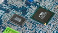
The THCS251 from THine is a transceiver IC that integrates both a common mode logic (CML) serializer and a deserializer into a single chip. THine states that a pair of THC251s enable up to 37 independent data flows to be transmitted and received over two differential pairs.

The THine THCS251. Image used courtesy of THine
The GPIO/LVCMOS transceiver IC’s signal path is supported by 8B10B encoding and built-in adaptive equalization. This allows it to transmit and receive high-speed signals over distances of 15 meters and more.
Key Features
General Purpose I/O (GPIO) clocking can be affected by an internal clock. It can also employ an external reference with acceptable frequencies ranging from 9 MHz to 133.3 MHz.

Block diagram of the THCS251. Image used courtesy of THine
The unit consumes 3 mA in sleep mode. There is also a standby mode that supports 8-bits low-speed GPIO. Standby mode consumes 4 mA.
In full-duplex bi-directional mode, the THCS251 supports a maximum total bandwidth of 4.67 Gbps.
THCS251 IC Solves the Hinge Problem
Laptops use hinges to connect the display to the rest of the device. Devices such as surveillance cameras, which require full 360-degree rotation, employ slip rings.
These slip rings and hinges, because of constraints imposed by both space and cost, limit the number of signal-carrying wires passing through them.
At the same time, while the number of signal-carrying lines must, by mechanical necessity, be decreased, the demand for greater and more sophisticated I/O is increasing for better user experiences. Thus, aggregation of those ever-increasing numbers of data pathways allows more flexible implementations that can reduce product size and cost.

Application of the THCS251, which is geared to reduce both cost and BOM count, while increasing reliability. Image used courtesy of THine
“This IC can be a game-changer for many applications,” explains Tak Iizuka, THine's chief solution architect. “Hinges used in many devices cause product limitations. For example, even the wide hinges used in laptops limit the number of wires to 15 per hinge.”
The THCS251 can serialize up to 37 lines into a pair of differential signals and then de-aggregate the differential signals back to the original 37 lines. As such, using one THCS251 on each side of the hinge or slip ring connector can reduce the number of wires coursing around a slip ring or hinge.
This will empower designers to build new applications that require higher I/O counts while cutting down on the reliability issues that would otherwise be apparent.
Other Applications
The transceiver, due to its 15-meter range, is compatible with any system that must support many controls or data signals between separate subsystems.
These include TVs, surveillance cameras, robotics, medical equipment, extended reality (XR) and gaming systems, and multi-functional printers.
Physical Considerations
The THCS251 operates with a power supply voltage ranging from 1.7 V to 3.6 V. I/O voltage range is also 1.7 V to 3.6 V.
The operating temperature range is from -40℃ to 85℃.
The unit is available in a 9 mm x 9 mm 64-pin QFN package.