Facebook
 Google
 GitHub
 Linkedin
An Arduino-Compatible Joystick Interface for RS-485 Motion Control
This project brief describes how to build and use an Arduino-compatible interface board that reads a 2-axis thumb joystick and transmits its position over an RS-485 network.
This board is built around an ATmega328 microcontroller and an SN65HVD08DR half-duplex RS-485 transceiver. A 2-axis, 10 kΩ thumb joystick with an integrated tactile switch is mounted directly on the board, along with header connectors for general-purpose I/O and a footprint for an optional 0.96-inch OLED display. Screw terminals bring out the RS-485 A and B lines for the twisted-pair bus cable, and the remaining I/O signals are available on pin headers for expansion (Figure 1).
The ATmega328 samples the joystick's two analog axes and its pushbutton, then formats the readings for transmission over the RS-485 bus. Typical applications include crane control, camera pan-tilt head positioning, and joystick-based motion control for equipment that needs to be operated over a long, noise-resistant serial link.
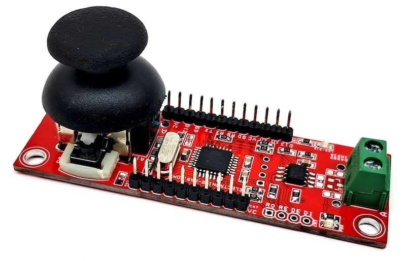
Figure 1. The assembled RS-485 joystick interface board.
Specs and Features
- Supply voltage: 5 V DC
- 2-axis thumb joystick, 10 kΩ, with integrated tactile pushbutton switch
- Half-duplex RS-485 communication (SN65HVD08DR transceiver)
- Screw terminal for RS-485 A/B connection
- Multiple Arduino I/O lines broken out to headers
- On-board power LED and function LED (tied to D13)
- Optional 0.96-inch OLED display footprint
- Optional 433 MHz RF module footprint
- Four 3 mm mounting holes
- PCB dimensions: 78.74 x 26.51 mm
How It Works
The ATmega328 reads the joystick's two potentiometers on its analog inputs and the pushbutton on a digital I/O pin, then drives the SN65HVD08DR transceiver to send the position data out over RS-485. The transceiver connects to the microcontroller as follows:
- RO (Receiver Output) = Arduino D10
- RE (Receiver Enable) = Arduino D2
- DE (Driver Enable) = Arduino D3
- DI (Driver Input) = Arduino D11
The SN65HVD08DR combines a three-state differential line driver and receiver in a single SOIC-8 package, compliant with the ANSI TIA/EIA-485-A and ISO-8482E standards. It operates from a 3 V to 5.5 V supply, draws less than 90 mW of quiescent power, and includes open-circuit, short-circuit, and idle-bus failsafe biasing on the receiver. Its driver output slew rate is limited for clean signal quality at data rates up to 10 Mbps, and its bus pins tolerate ESD events above 16 kV (HBM), making it a rugged choice for an RS-485 node that may see long cable runs or a noisy electrical environment.
An optional 0.96-inch OLED display can be soldered to the underside of the board over the I2C header for local status readout, and an optional 433 MHz RF module footprint is provided for wireless retransmission of the joystick data. The included test firmware transmits joystick position over RS-485; the matching RS-485 relay driver board (published separately) can receive it, trigger a threshold, and drive a relay in response.
Schematic and Bill of Materials
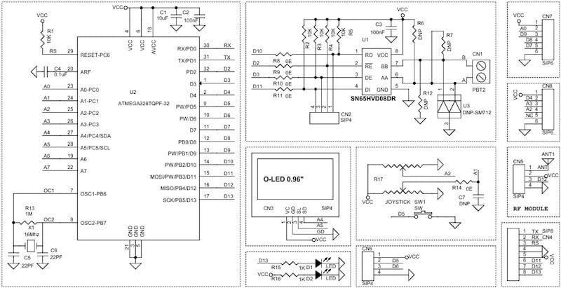
Figure 2. Schematic for the RS-485 Joystick Interface Board.
The bill of materials is shown in Table 1.
Table 1. BOM for RS-485 Joystick Interface Board.
| REF | DESCRIPTION | QTY | MFG | SUPPLIER | PART NO. |
| ANT1 | Antenna (optional, not populated) | 1 |
|
|
|
| CN1 | 2-pin screw terminal, 5.08 mm pitch | 1 | Phoenix | Digi-Key | 277-1247-ND |
| CN2, CN3, CN5, CN6 | 4-pin male header, 2.54 mm pitch | 4 | Würth | Digi-Key | 732-5317-ND |
| CN4 | 8-pin male header, 2.54 mm pitch | 1 | Würth | Digi-Key | 732-5321-ND |
| CN7 | 6-pin male header, 2.54 mm pitch | 1 | Würth | Digi-Key | 732-5319-ND |
| CN8 | 6-pin connection pad, underside of PCB | 1 |
|
|
|
| C1 | 10 µF / 16 V ceramic, 0805 | 1 | Yageo/Murata | Digi-Key |
|
| C2, C3, C4 | 100 nF / 50 V ceramic, 0805 | 3 | Yageo/Murata | Digi-Key |
|
| C5, C6 | 22 pF / 50 V ceramic, 0805 | 2 | Yageo/Murata | Digi-Key |
|
| R6, R7, C7, R12 | Do not populate | 4 |
|
|
|
| D1, D2 | Red LED, SMD 0805 | 2 | OSRAM | Digi-Key | 475-1278-1-ND |
| R1, R2, R3, R4, R5 | 10 kΩ 5%, SMD 0805 | 5 | Yageo/Murata | Digi-Key |
|
| R8, R9, R10, R11, R14 | 0 Ω 5%, SMD 0805 | 5 | Yageo/Murata | Digi-Key |
|
| R13 | 1 MΩ 5%, SMD 0805 | 1 | Yageo/Murata | Digi-Key |
|
| R15, R16 | 1 kΩ 5%, SMD 0805 | 2 | Yageo/Murata | Digi-Key |
|
| R17 / JOY1 | 2-axis thumb joystick, 10 kΩ | 1 | C&K | Digi-Key | 108-THB001P-ND |
| U1 | SN65HVD08DR, SOIC-8 | 1 | TI | Digi-Key | 296-39173-1-ND |
| U2 | ATmega328, TQFP-32 | 1 | Microchip | Digi-Key | ATMEGA328-AU-ND |
| U3 | SM712, do not populate | 1 |
|
|
|
| X1 | 16 MHz crystal | 1 | ECS Inc. | Digi-Key | X1103-ND |
Connections
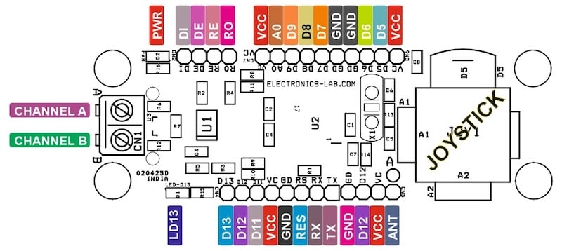
Figure 3. Connector and pinout map for the joystick interface board.
CN1 — RS-485 Bus (2-pin screw terminal):
- Pin 1 = RS-485 Channel B
- Pin 2 = RS-485 Channel A
CN2 — Optional, not used
CN3 — 0.96-inch OLED Display Header (optional)
CN4 — Bootloader/Programming Port (8-pin):
- Pin 1 = TX
- Pin 2 = RX
- Pin 3 = Reset
- Pin 4 = GND
- Pin 5 = VCC
- Pin 6 = D11
- Pin 7 = D12
- Pin 8 = D13
CN5 — 433 MHz RF Module Header (optional)
CN6 — I/O Header (4-pin):
- Pin 1 = VCC
- Pin 2 = D5
- Pin 3 = D6
- Pin 4 = GND
CN7 — I/O Header (6-pin):
- Pin 1 = VCC
- Pin 2 = A0
- Pin 3 = D9
- Pin 4 = D8
- Pin 5 = D7
- Pin 6 = GND
CN8 — I/O Pad, Underside of PCB (6-pin):
- Pin 1 = VCC
- Pin 2 = D4
- Pin 3 = A3
- Pin 4 = A2
- Pin 5 = NC
- Pin 6 = GND
JOY1 / R17 — 2-Axis Thumb Joystick, 10 kΩ:
- X-axis output to Arduino A1
- Y-axis output to Arduino A2
- Integrated pushbutton switch to D5
D1 — Function LED, tied to D13
D2 — Power LED
PCB Files
Figure 4 shows the PCB layout, top and bottom copper layers, and board dimensions.
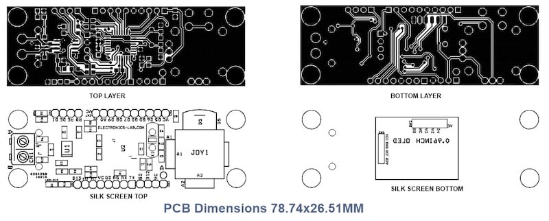
Figure 4. PCB layout for the joystick interface board, 78.74 x 26.51 mm.
You can download the layout files for this project here:
RS-485 Joystick Interface Gerber Files
Except where noted, all images used courtesy of Rajkumar Sharma
Related Content