 Facebook
 Google
 GitHub
 Linkedin
Build Your Own Motion Detection System Using an Accelerometer
This project uses a C8051 microcontroller development kit, an accelerometer evaluation board, and Simplicity Studio IDE—all from Silicon Labs—to rather quickly and easily build a motion-detecting alarm system.
This project uses a C8051 microcontroller development kit, an accelerometer evaluation board, and Simplicity Studio IDE—all from Silicon Labs—to rather quickly and easily build a motion-detecting alarm system.
C8051F930 Development Kit
The C8051F930 development kit is intended as a development platform for the microcontrollers in the C8051F93x-C8051F92x MCU family. This kit comes with the C8051F930 microcontroller installed—see Figure 1 below.
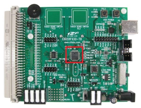
Figure 1. C8051F930 development kit. C8051F930 microcontroller (red box).
The C8051F930 microcontroller includes the following features:
- Single supply: 0.9 to 3.6V
- High-speed 8051 µC core
- 10-bit ADC
- 4352 bytes internal data RAM
- 64kB Flash memory
- 24 port I/Os
- SMBus, I2C, 2x SPI, UART
- On-chip debug
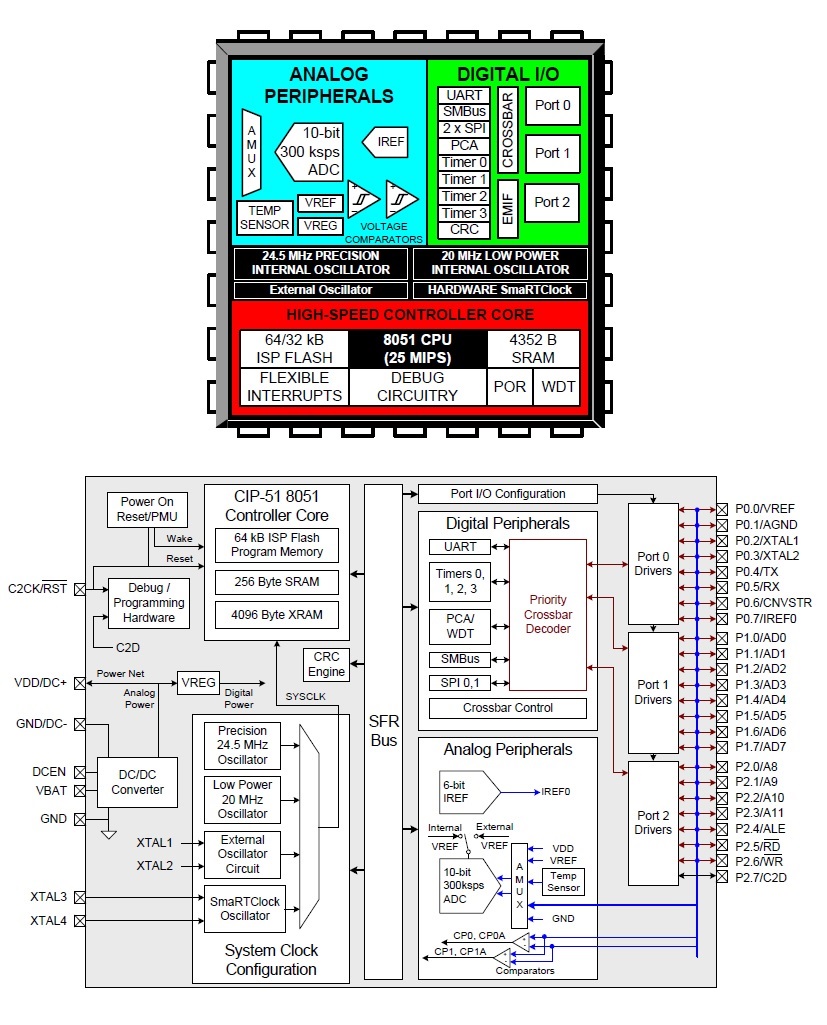
Figure 2. C8051F930 block diagrams
Other microcontrollers in the C8051F93x-C8051F92x family have less Flash memory and/or fewer I/Os than the C8051F930.
The Silicon Labs IDE, called Simplicity Studio, is available as a free download, and it includes example code.
Accelerometer Evaluation Board
At the core of the accelerometer evaluation board (STEVAL-MKI135V1) is the accelerometer device itself (LIS2DH), which has features including:
- ultra low-power
- three-axis device
- digital I2C/SPI serial interface
- dynamically user selectable full scales of ±2g/±4g/±8g/±16g
- may be configured to generate up to two interrupt signals based on:
- detection of movement (user-selectable threshold)
- detection of no movement (user-selectable threshold)
- free-fall event
.jpg)
Figure 3. Accelerometer evaluation board.
Audio Alarm
The audio piezo alarm chosen for this project is a slow warble alarm with a resonant frequency range of 2500 to 3500 Hz. Given its relatively small size, this bugger generates an ear piercing sound of 100dB at 100cm (with a drive voltage of 12V). This alarm has its own internally driven circuitry and operates from 5V to 15V, which is perfect for this project because we have 12V readily available. Just apply the voltage and you're off and running—no worrying about feeding the alarm a PWM signal for the warble effect.

Figure 4. Audio alarm
LED Flood Lights
The reason I chose these particular LED flood lights is simply because I had them in my lab. Also, they're convenient components for this 12V system because they operate from a 12V supply.

Figure 5. 12V LED flood light
Parts List
| Item # | Description / Source | Cost (each) | Other Information |
|---|---|---|---|
| 1 | C8051F930 development kit | $99.00 | User guide Quick-start guide C8051F930 datasheet Note: schematics are on pages 23-25 of the User Guide. |
| 2 | Breadboard | $8.98 | or equivalent |
| 3 | Jumper wire kit | $5.28 | or equivalent |
| 4 | Accelerometer evaluation board (STEVAL-MKI135V1) |
$21.28 | Evaluation board datasheet Device datasheet |
| 5 | Audio alarm | $6.08 | Datasheet |
| 6 | LED flood light (qty 2) | $10.29 | 10W; 12V DC or AC |
| 7 | N-Channel MOSFETs (qty 2) | $1.17 | Datasheet or equivalent |
Connecting the Components
The microcontroller configures the accelerometer—using the SPI protocol—to detect very slight accelerations in the X- and Y-axes. When an acceleration is detected in either axis, the accelerometer generates an interrupt signal that is detected by the microcontroller. After receiving the interrupt signal, the microcontroller then turns on two external FETs thereby energizing both the audio alarm and the two LED flood lights. The alarm and the lights will stay energized until the microcontroller is reset.
Before energizing the microcontroller development kit, be sure to configure it as follows:
Jumpers:
- J11: VBAT to WALL_PWR
- J12: VDD to VIO
- J17: VBAT_PIN to VBAT
Switches:
- SW4: set to "2 CELL"
- Important Note: According to the User's Guide, the power switch (SW5) must be in the OFF position prior to switching between one-cell and two-cell mode using SW4.
- The power options are described in section 5.2.1 of the User's Guide.
- Power switch (SW5) to "OFF" position—we'll change this later on
Cables:
- Connect the ribbon cable debug adapter to J9
- Connect the USB debug adapter to your PC
- Connect the supplied AC/DC power adapter to P2
Breadboard the Components
Figure 7 below depicts the connections between the various components. As can be seen, the two N-Channel FETs behave as low-side switches: when the FETs' gates are pulled high (3.3V), the FETs allow current to flow from drain to source. The 4-wire SPI connection between the accelerometer and the microcontroller is also shown.

Figure 6. Depiction of how the components should be connected together
Once the components are all connected, it's time to write firmware.
Writing Firmware Using Simplicity Studio
Using the Simplicity Studio IDE is straightforward. Before running Simplicity Studio IDE, make sure your development kit is connected to your PC and powered up.
Once the IDE is running it should automatically find your C8051F930 evaluation kit. If not, then type "C8051F930" in the product field on the left-hand side of the screen. The C8051F930 Development Kit should become visible as an option—click on this option (see Figure 8 below).

Figure 7. Choosing the correct C8051 product.
After Simplicity Studio has C8051F930 Development Kit shown as the Current Product, then navigate to F93x-92x ADC0 ExternalInput under "Software and Kits" and "Software Examples". See Figure 9 below.

Figure 8. Choosing the correct example code.
On the Project Configuration screen, leave everything as is (see Figure 9 below) then click Finish. The IDE will appear with the "F93x_ADC0_ExternalInput.c" file open. The code is well commented.

Figure 9. Project configuration.
Now that the example code has been loaded, we need to make the following modifications—for these changes, it's best (and easiest) to use the F93x_ADC0_ExternalInput.hwconf file.
- Port 1.2 (this port is associated with the Int1 signal from the accelerometer):
- Change Skip: from Not Skipped to Skipped
- Port 2.1 (this port is used to control the FETs):
- Change Drive Strength: from Low to High
- Change IOMode: from Digital OpenDrain I/O to Digital Push-Pull Output.
- Change Latch: from High to Low
- Change Skip: from Not Skipped to Skipped
- SPI0
- Change Clock Phase: from Data sample on first edge to Data sample on second edge.
- Change Clock Polarity: from Low in idle state to High in idle state.
Tip: During the development of this project I got hung up on the Clock Phase and Clock Pulse configurations. Although not clearly called out in the accelerometer datasheet, they are mentioned. However, instead of referencing "Clock Phase" and "Clock Polarity"—which seems to be the norm (see section 24.5 of the C8051F930 datasheet)—the accelerometer LIS2DH datasheet (see page 26) simply states: "SPC is the serial port clock and it is controlled by the SPI master. It is stopped high when CS is high (no transmission). SDI and SDO are respectively the serial port data input and output. Those lines are driven at the falling edge of SPC and should be captured at the rising edge of SPC."
In reality, this issue had me stumped before I resorted to utilizing an SPI bus analyzer. Figure 10 below is a screen shot of said analyzer with the correct configuration.
If you run into any SPI bus issues or if your accelerometer device—or any other SPI or I2C device on other projects—isn't working as expected, I highly recommend that you consider buying an SPI bus analyzer. The one I use is a Saleae Logic Analyzer (24MHz, 8-channel).

Figure 10. SPI bus analyzer with the correct clock phase and clock polarity settings.
Once you have completed the configuration changes to the microcontroller, you'll have to add all the code to correctly configure the accelerometer. This must be added to the F93x_SPI0_Master.c file. The code excerpt below shows the necessary code changes.
	//	The accelerometer requires 5ms for booting after power is applied.
	Delay ();

	//	Assign the address of the desired register within the accelerometer:
	//	Address to write = 0x60 --> 0x20 for CTRL_REG1[20h] + 0x40 for RW# (bit 7) = 0, and MS# (bit 6) = 1
	//	Reference section 5.2.2 of LIS2DH accelerometer datasheet for more information on RW# (bit 7) and MS# (bit 6).
	SPI_Data_Array[0]=0x60;
	SPI_Data_Array[1]=0x73; // CTRL_REG1[20h]: 400 Hz Normal Mode. X- and Y-axis enabled.
	SPI_Data_Array[2]=0x00; // CTRL_REG2[21h]: High-pass filter disabled.
	SPI_Data_Array[3]=0x40; // CTRL_REG3[22h]: Interrupt activity driven to INT1.
	SPI_Data_Array[4]=0x00; // CTRL_REG4[23h]: FS = +/-2 g
	SPI_Data_Array[5]=0x00; // CTRL_REG5[24h]: Interrupt pin not latched.
	SPI_Data_Array[6]=0x02; // CTRL_REG6[25h]: Active Low

	// Assign the number of bytes in the array "SPI_Data_Array" that are to be sent to the accelerometer.
	BytesToSend = 7;

	// Send the array data to the slave (i.e., accelerometer).
	SPI_Array_Write ();		// Send the array data.

	//	Assign the address of the desired register within the accelerometer:
	//	Address to write = 0x70 --> 0x30 for INT1_CFG[30h] + 0x40 for RW# (bit 7) = 0, and MS# (bit 6) = 1
	SPI_Data_Array[0]=0x70;
	SPI_Data_Array[1]=0x0A;		// INT1_CFG[30h]: Enable XH and YH interrupt generation, and enable OR combination of interrupt events.

	// Assign the number of bytes in the array "SPI_Data_Array" that are to be sent to the accelerometer.
	BytesToSend = 2;

	// Send the array data to the slave (i.e., accelerometer).
	SPI_Array_Write ();		// Send the array data.

	//	Assign the address of the desired register within the accelerometer:
	//	Address to write = 0x72 --> 0x32 for INT1_THS[32h] + 0x40 for RW# (bit 7) = 0, and MS# (bit 6) = 1
	SPI_Data_Array[0]=0x72;
	SPI_Data_Array[1]=0x10; // INT1_THS[32h]: Threshold 256 mg.  0x10 -->  16LSBs * 16mg/LSB [at FS=2g] = 256mg.

	// Assign the number of bytes in the array "SPI_Data_Array" that are to be sent to the accelerometer.
	BytesToSend = 2;

	// Send the array data to the slave (i.e., accelerometer).
	SPI_Array_Write ();		// Send the array data.

	while (1)
	{
		if(P1_B2 == 0)		// If Accelerometer is moving. Accelerometer Interrupt is Active Low
		{
			LED = LED_ON;
			ALARM = ALARM_ON;
			while (1)
			{
				        // Wait here forever.
			}
		}
		else if (P1_B2 == 1)	// If Accelerometer is NOT moving. Accelerometer Interrupt is Active Low
		{
			LED = LED_OFF;
			ALARM = ALARM_OFF;
		}

	}
As can be seen, I have configured register 0x20 in such a way that only the X and Y axes are enabled. Register 0x32 sets the acceleration threshold (set to 256mg) for when the Int1 signal is driven; the 256mg threshold setting is what makes the motion detector so sensitive to slight accelerations.
All the code for this project can be downloaded from the link below.
Accelerometer_Motion_Detector_Audio-Alarm_Lights.zip
Building and Loading the Code ... and Testing the System
Once all the code has been modified, build the project and download the code to the microcontroller. Be sure to have the accelerometer on a fairly level surface. After you run the code, lightly tapping the accelerometer evaluation board (or the breadboard) should sound the alarm and turn on the two LED flood lights.
In the video demonstration below, you can see that tapping the breadboard triggers the alarm, and pressing the development board's reset button re-arms the system.
Summary and Next Steps
As demonstrated in this article, programming the C8051F930 microcontroller to configure and use the STEVAL-MKI135V1 accelerometer is quite straightforward—after, or course, you have mastered the Clock Polarity and Clock Phase configuration settings.
If you decide to use this accelerometer in a new design—sans the development and evaluation boards—you'll want to use the LIS2DH accelerometer device itself on your new PCB design. Be sure to pay close attention to the part's layout requirements as this device is quite small, with its pads being much, much smaller. ST has provided Gerber files, schematics, and a BOM that you may want to use as a reference guide.
Good luck!
Give this project a try for yourself! Get the BOM.
Related Content


Cool looking project. However, when you said “motion detector” I was thinking “infrared” not “vibration”. So you’ve created the equivalent of a Minecraft pressure plate, here?
https://minecraft.gamepedia.com/Pressure_Plate
😊