Facebook
 Google
 GitHub
 Linkedin
PWM Digital-to-Analog Conversion with the SAM4S Xplained Pro
In this article we’ll use the SAM4S Xplained Pro development platform to get some hands-on experience with a PWM DAC.
In this article, we’ll use the SAM4S Xplained Pro development platform to get some hands-on experience with a PWM DAC.
Supporting Information
- Intro to Project Development with the Atmel SAM4S Xplained Pro
- Turn Your PWM into a DAC
- Low-Pass Filter a PWM Signal into an Analog Voltage
Required Hardware/Software
- SAM4S Xplained Pro evaluation kit
- I/O1 Xplained Pro extension board, or you can connect your own low-pass filter to the appropriate header pins
- Atmel Studio
Previous Article
Pins and Signals and Probes, Oh My
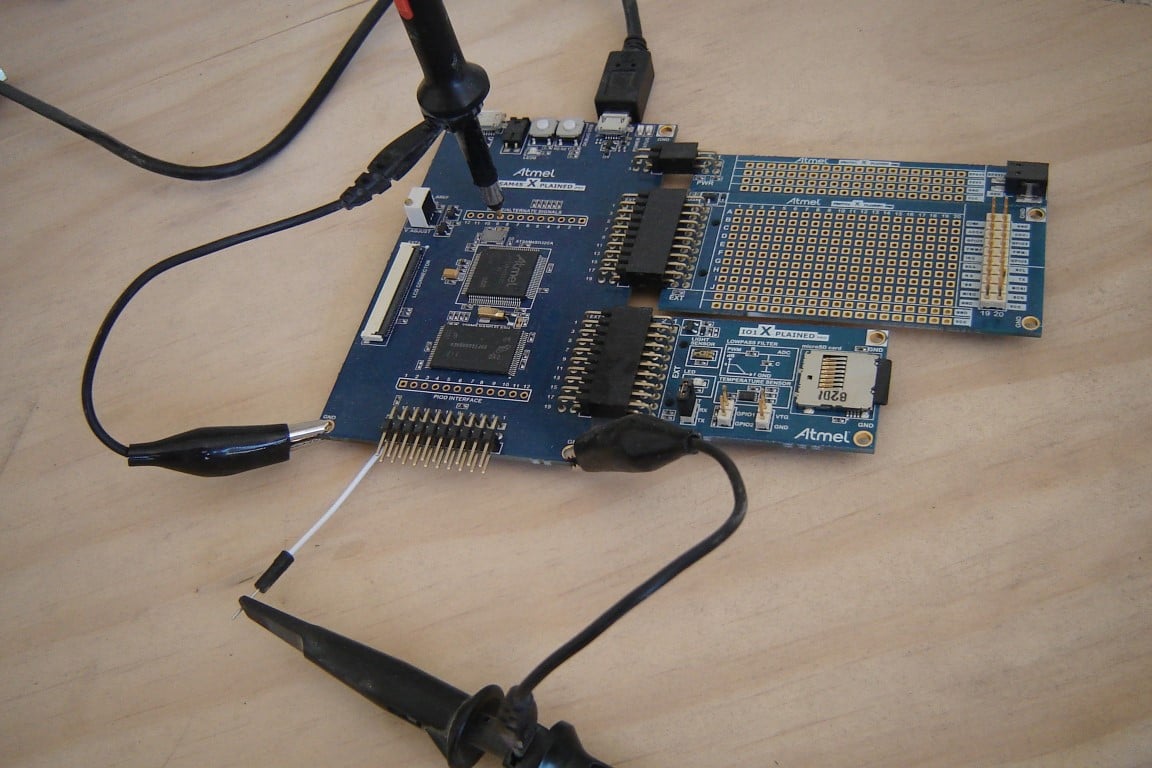
In the previous article we solidified our control over the SAM4S PWM hardware, bending it to our will by means of the Atmel Software Framework (ASF). Now we are ready to make the PWM hardware do something useful—namely, generate a programmable analog voltage with the help of nothing more than an RC low-pass filter. The first thing we need to do is iron out the details with our hardware setup. We will use oscilloscope measurements to observe and analyze the PWM and DAC waveforms, so an important part of this setup is how to conveniently probe the relevant signals.
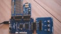
If you have the I/O1 extension board, you can replicate my hardware setup:
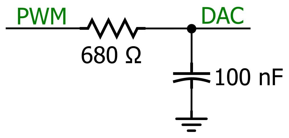
Low-pass filtering is achieved by the RC filter on the I/O1 board. It just so happens that the input to this RC filter is connected to a PWM pin on the SAM4S microcontroller, and furthermore the RC filter is complemented by a nifty little silkscreened Bode plot—nice touch, Atmel. The cutoff frequency is approximately 2340 Hz.
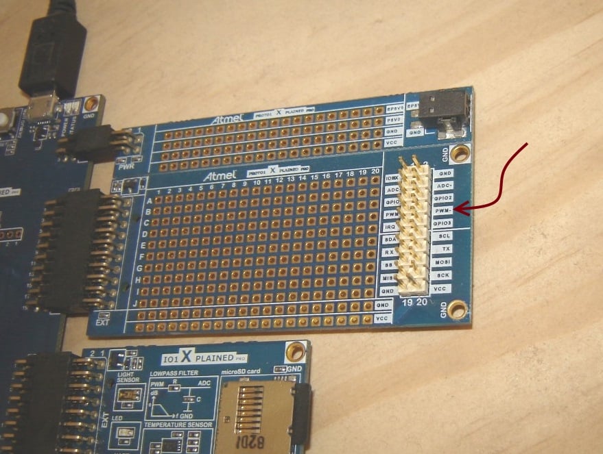
The I/O1 board does not include individual headers for the low-pass filter’s input and output signals, so we need to find another way to attach the probes. The 20-pin EXT header would be convenient if the relevant signals were connected to odd-numbered pins, but as luck would have it they are both even-numbered, and the even-numbered pins are not accessible:
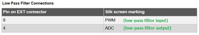
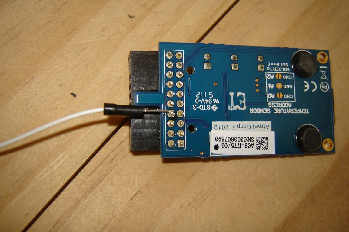
Fortunately, one of these signals is available elsewhere. The low-pass filter output is connected to pin PB1, which is also available from terminal 9 in the row of through-holes labeled “SPARE/ALTERNATE SIGNALS” on the SAM4S development board. This is why the above photo shows one of the probes lodged in spare/alternate number 9. There is no convenient access to the low-pass filter input node, so I soldered a jumper wire to pin 8 on the I/O1 EXT header, as follows:
The only annoyance with my setup is the jumper wire. If you don’t like soldering or don’t have an iron at your disposal, here is an alternative: The low-pass filter input on the I/O1 board is connected to the negative (i.e., inverted) output from PWM channel 1. On the PROTO1 board (shown in the above photo), you can easily probe the negative output from PWM channel 0, because it is right there on the prototyping header:
So instead of probing the actual input to the low-pass filter, you simply probe PWM0– on the PROTO1 board then modify the code so that PWM channels 0 and 1 are both enabled and are always generating the same PWM signal (same clock source, same period, same duty cycle, etc.).
Finally, if you don’t have the I/O1 board, you can use the PROTO1 board, a breadboard, or some sort of jury-rigged direct-solder implementation to get a low-pass filter connected to one of the PWM signals. If you use the PROTO1 board, plug it into EXT2 so that you don’t have to modify the code (EXT1 and EXT2 have different PWM signals—channel 0 for EXT1 and channel 1 for EXT2). This is the low-pass circuit used on the I/O1 board:
Accuracy and Ripple
Here is a basic code framework for PWM digital-to-analog conversion:
#include

#define PWM1L_DAC IOPORT_CREATE_PIN(PIOA, 20)

#define PWM_CLOCKSOURCE_FREQ 10000000
#define PWM_FREQ 100000
#define PWM_PERIOD_TICKS PWM_CLOCKSOURCE_FREQ/PWM_FREQ
#define MEASURED_VHIGH 3

float DAC_voltage = 1;

pwm_channel_t PWM1_config;

int main (void)
{
	//clock configuration and initialization
	sysclk_init();

	/*Disable the watchdog timer and configure/initialize
	port pins connected to various components incorporated
	into the SAM4S Xplained development platform, e.g., the
	NAND flash, the OLED interface, the LEDs, the SW0 pushbutton.*/
	board_init();

	//connect peripheral B to pin A20
	pio_configure_pin(PWM1L_DAC, PIO_TYPE_PIO_PERIPH_B);

	//enable the peripheral clock for the PWM hardware
	pmc_enable_periph_clk(ID_PWM);

	//disable the PWM channel until it is properly configured
	pwm_channel_disable(PWM, PWM_CHANNEL_1);

	//PWM clock configuration
	pwm_clock_t PWMDAC_clock_config =
	{
		.ul_clka = PWM_CLOCKSOURCE_FREQ,
		.ul_clkb = 0,
		.ul_mck = sysclk_get_cpu_hz()
	};

	//apply the clock configuration
	pwm_init(PWM, &PWMDAC_clock_config);

	//select channel 1
	PWM1_config.channel = PWM_CHANNEL_1;
	//select clock A
	PWM1_config.ul_prescaler = PWM_CMR_CPRE_CLKA;
	/*The low-pass filter is connected to the inverted output
	for PWM channel 1, so to get an active-high signal we
	invert again by setting the polarity to low.*/
	PWM1_config.polarity = PWM_LOW;
	//left-aligned mode
	PWM1_config.alignment = PWM_ALIGN_LEFT;

	PWM1_config.ul_period = PWM_PERIOD_TICKS;
	PWM1_config.ul_duty = (DAC_voltage * MEASURED_VCC) / PWM_PERIOD_TICKS;

	//apply the channel configuration
	pwm_channel_init(PWM, &PWM1_config);

	//configuration is complete, so enable the channel
	pwm_channel_enable(PWM, PWM_CHANNEL_1);

	while(1);
}
As you can see, we use preprocessor directives to define
- the frequency of the clock that drives the PWM hardware (i.e., clock A),
- the frequency of the PWM waveform,
- the period of the PWM waveform in units of clock A ticks, and
- the measured digital supply voltage.
Then we have a floating point variable, DAC_voltage, for the desired output voltage. We configure the PWM frequency by setting PWM1_config.ul_period equal to PWM_PERIOD_TICKS. The frequency of the PWM waveform (PWM_FREQ) does not influence the nominal DAC output voltage, but it does influence the amount of ripple—as discussed in Low-Pass Filter a PWM Signal into an Analog Voltage, higher PWM frequency leads to lower ripple because the low-pass filter can more effectively suppress the non-DC components of the signal. The only two factors that influence the nominal DAC voltage are the duty cycle and the amplitude (i.e., logic-high voltage minus logic-low voltage) of the PWM waveform. The amplitude is out of our control, so everything comes down to the duty cycle. We calculate ul_duty (which is the duration of the pulse, not the duty cycle) as follows:
PWM1_config.ul_duty = (DAC_voltage * MEASURED_VCC) / PWM_PERIOD_TICKS;
This little calculation simply ensures that the ratio of ul_duty to ul_period is the same as the ratio of desired DAC voltage to PWM amplitude. Here we are assuming that the measured supply voltage is the same as the amplitude, and we will soon see that this is our dominant source of error.
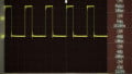
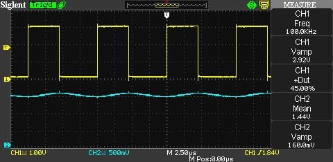
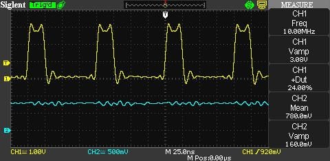
Here is a scope capture for the settings shown above (PWM frequency = 100 kHz, DAC_voltage = 1, PWM amplitude = 3.28 V):
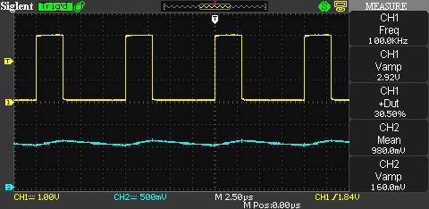
The salient measurements are displayed on the right-hand side. The frequency is as expected, and the duty cycle is consistent with the theoretical value: (1 V)/(3.28 V) = 0.305. The major discrepancy is the amplitude. The PWM waveform is switching from about 100 mV to 3 V, rather than 0 V to 3.28 V. Now here is an important detail: When the logic-low voltage is not at 0 V, the DAC voltage is no longer calculated as (PWM amplitude) × (duty cycle). Instead, we need to use
\[DAC\ voltage=\left(\left(V_{HIGH}-V_{LOW}\right)\times duty\ cycle\right)+V_{LOW}\]
Thus, the expected DAC voltage under the current conditions is
\[DAC\ voltage=\left(\left(3\ V-100\ mV\right)\times30.5\%\right)+100\ mV=985\ mV\]
And this is almost exactly what the scope calculated as the average value of the DAC voltage. So keep in mind that you cannot simply multiply the scope’s “CH1 Vamp” by “CH1 +Dut” to determine the expected output voltage; you need to take the result of this multiplication and add it to the PWM signal’s actual logic-low voltage. In any event, we have ~20 mV of error in the average DAC voltage resulting from the discrepancy between the assumed logic-high and -low voltages and the real logic-high and -low voltages. As for the ripple, we’re looking at about 150 mV peak-to-peak. (The scope has trouble with this measurement because of the noise spikes that occur at the same time as the logic transitions in the PWM waveform. These are the result of crosstalk between the two scope channels; they’re not actually present in the DAC signal.) With 150 mV of ripple and 20 mV of error, my general conclusion so far is that we have a DAC here; it’s not impressive, but if this sort of performance is adequate for your application, it’s cheaper and simpler than an external DAC.
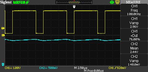
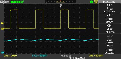
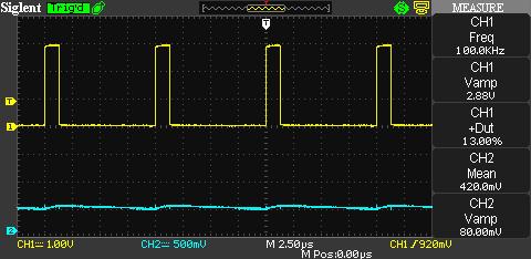
Here are scope captures for DAC_voltage = 0.5, 1.5, and 2.5:

Improvements
What can we do to make this PWM DAC a little less mediocre? Our two major problems are ripple and error. The ripple is fairly easy to reduce: as mentioned above, we just increase the frequency of the PWM waveform. The error is more problematic; the best solution is to buffer the PWM signal so that the logic-high and logic-low voltages are closer to VCC and ground. But a buffer chip falls into the same category as a higher-order low-pass filter—if you go beyond the basic PWM-plus-RC-filter implementation, you might as well just use an external DAC. So instead of a buffer we will simply modify our calculations to account for the PWM signal’s actual high and low voltages. This may seem like cheating, but it actually is a good design technique: If you’re working with a one-off system, it makes sense to modify the code in accordance with some basic measurements. If you’re working with a prototype system that will be produced in large quantities, it makes sense to base performance assumptions on your experience with the prototype. Sure, the high and low voltages might vary significantly from one unit to another; but then again, they might not. In any event, there’s not much point in basing the calculations on VCC and ground, because in general a microcontroller’s output stage will not drive a signal all the way up to VCC or all the way down to ground.
So let’s modify the code according to the logic-high and logic-low measurements given above, namely, VHIGH = 3 V and VLOW = 100 mV.
#define MEASURED_VHIGH 3
#define MEASURED_VLOW 0.1

. . .

PWM1_config.ul_duty = ((DAC_voltage - MEASURED_VLOW) / (MEASURED_VHIGH - MEASURED_VLOW)) * PWM_PERIOD_TICKS;
And here are the results with DAC_voltage = 1.
Hey, the error is zero! Success! Oh wait, here are the results for DAC_voltage = 0.5 and DAC_voltage = 2.5.

Sigh. So even variations in PWM duty cycle can lead to enough change in the high and low voltages to cause significant error. This brings up the idea of a more sophisticated scheme in which the calculation uses different high and low voltages depending on the duty cycle, but I would use an external DAC before I devoted much time to that.
At least we know that we can improve the ripple. Let’s increase the PWM clock source frequency to 120 MHz and the PWM frequency to 10 MHz. Here are scope captures for DAC_voltage = 1. The PWM probe is disconnected for the second capture so that we can see what the DAC waveform looks like without the crosstalk (though there still seems to be some noise coupling into the DAC signal).
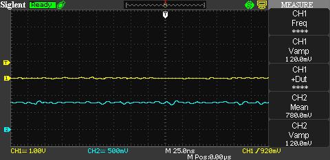
The higher frequency reduces the ripple to negligible levels, but the high and low voltages have changed enough to introduce a large amount of error (recall that the error was zero when we were using the lower frequency with DAC_voltage = 1).
Conclusion
You can use the following link to download the source and project files:
We have seen that PWM DACs suffer from serious limitations. In addition to the error and ripple discussed above and the long settling time discussed in Low-Pass Filter a PWM Signal into an Analog Voltage, the available resolution decreases as PWM frequency increases—though the PWM uses a 16-bit counter, higher frequencies reduce the usable width of that counter because both the period and the pulse width are determined by registers that are compared to the same counter. For example, if the PWM counter resets at 100 because it must generate a 100 µs period from a 1 MHz clock, the duty cycle register cannot exceed 100, resulting in resolution of less than 7 bits (because 27 = 128). The bottom line: if you can tolerate the limitations, a PWM DAC is a simple, low-cost solution, but most of the time you are better off with a normal DAC, whether external or integrated into a microcontroller.
Give this project a try for yourself! Get the BOM.
Related Content