Facebook
 Google
 GitHub
 Linkedin
Analog Design Trade-Offs in Applying Linearization Techniques Using Example CMOS Circuits
This article will look at the trade-offs we face when trying to improve the linearity of a circuit.
Digital integrated circuit design usually involves optimizing three different parameters: speed, occupied silicon area, and power consumption. However, in analog design, we have to consider several other aspects of the circuit performance such as linearity, noise, input/output impedance, stability, and voltage swings. There are usually trade-offs between these parameters and we cannot improve all of them simultaneously. This article will look at the trade-offs we face when trying to improve the linearity of a circuit. We’ll see that circuit linearity usually trades with gain, noise, and speed. We’ll examine simple CMOS analog circuits to gain intuition into these trade-offs.
The Origin of Non-Linearity
Linearity performance determines the largest signal that the circuit can process with an acceptable accuracy. With a large input signal, the circuit parameters can significantly change with the instantaneous amplitude of the input. For example, consider the common-source amplifier shown in Figure 1.
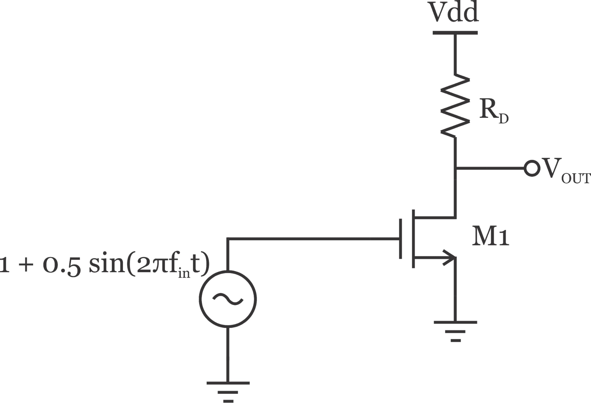
Figure 1. A common-source amplifier circuit
Ignoring the output resistance of the transistor, the voltage gain of this circuit is \(g_{m1}R_D\) where \(g_{m1}\) denotes the transistor transconductance. Considering the square-law model for the MOS transistor, we have:
\[g_{m1}=k' \frac {W}{L}(V_{GS}-V_{th})\]
where k' is a process-dependent parameter and \(\frac {W}{L} \) specifies the size of the transistor. In this equation, \(V_{GS}\) and \(V_{th}\) are the transistor gate-source voltage and threshold voltage, respectively. The above equation shows that \(g_{m1} \), and consequently the gain, depends on the transistor gate-source voltage. With the example depicted in figure 1, \(V_{GS}\) changes from 0.5 V to 1.5 V. Therefore, the circuit will exhibit a higher gain as we approach the peak of the input. (We assume that the output is not saturated because of the available voltage swing at the transistor drain. With a sufficiently large \(V_{GS}\), the DC value of the output will be close to ground and we’ll have a very limited swing at the output. In this case, the gain can actually decrease with an increase in \(V_{GS}\)). The input-dependent variation of gain is the origin of the circuit’s non-linearity. Note that, as we increase the amplitude of the input, the circuit becomes more and more non-linear. We discussed in a previous article on SFDR that circuit non-linearity can lead to several different frequency components at the output even if the input is a single-tone sinusoid. Now, let’s look at the common trade-offs we face when trying to improve the linearity of a circuit.
Speed-and-Linearity Trade-off
One common method to linearize a circuit is the negative feedback technique illustrated in Figure 2.
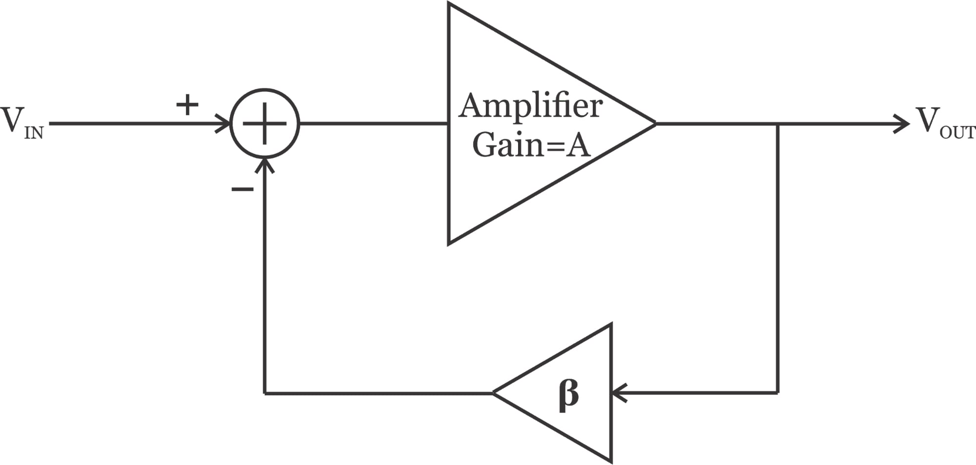
Figure 2. The negative feedback technique of circuit linearization.
The closed-loop gain of this circuit is given by:
\[\frac {V_{OUT}}{V_{IN}}= \frac {A}{1+ \beta A}\]
Equation 1
Assuming that \(\beta A \gg 1\), we have
\[\frac {V_{OUT}}{V_{IN}} \simeq \frac {1}{\beta}\]
The feedforward amplifier is implemented using transistors and can have input-dependent behavior similar to the single-stage amplifier discussed in the previous section. In other words, the value of A can change significantly with the input amplitude. However, the feedback path \((\beta)\) is usually implemented using passive elements such as resistors and capacitors. Passive elements are much more linear than active elements, and we can assume that \(\beta\) is independent of the input amplitude. Without applying the negative feedback technique, the gain (A) could change with the input and we would have a non-linear system. However, the closed-loop gain \(\left ( \frac {1}{\beta} \right )\) is constant ( assuming that \(\beta A \gg 1\)).
What is the cost of this improvement? Circuit linearity usually trades with gain, noise, speed, and power consumption. One of the important trade-offs that can be observed in a feedback-based linearization technique is the speed-and-linearity trade-off. Let’s look at this trade-off in greater detail. With an open-loop system, we don’t have to worry about stability. The system may introduce a delay from its input to the output and, as we increase the input frequency, the delay will increase. However, the introduced delay will not probably cause a serious problem. This is not the case for a closed-loop system where we have to carefully consider the loop delay because a sufficiently large phase shift can effectively make the feedback positive. Usually, increasing the input frequency of an amplifier reduces its gain and increases its phase shift. If the input frequency is increased sufficiently, the phase shift of the loop can approach \(180^\circ (\measuredangle \beta A=180^\circ)\), and the loop gain may still be greater than \(1 (\left | \beta A \right |>1)\), leading to instability. (See AAC’s article on negative feedback stability for more information.)
To make the closed-loop system stable, we have to apply frequency compensation techniques to sufficiently reduce the loop gain \((\left | \beta A \right |)\) to below 1 when the loop phase shift \((\measuredangle \beta A)\) is 180°. This is conceptually equivalent to placing a low-pass filter in the loop. Low-pass filters suppress high-frequency signals, therefore, we expect the operation frequency of the closed-loop system to be much more limited than that of the original uncompensated amplifier. To summarize, applying negative feedback increases linearity at the cost of reducing the frequency of operation.
Gain-and-Linearity Trade-off
A basic linearization technique is source degeneration. As depicted in Figure 3, this technique places a linear resistor \((R_S)\) at the source of the transistor. Note that we can consider this circuit as a structure with “local feedback” that samples the drain current and feeds back a proportional voltage in series with the input voltage. Hence, it should come as no surprise that the source degeneration increases the circuit linearity.
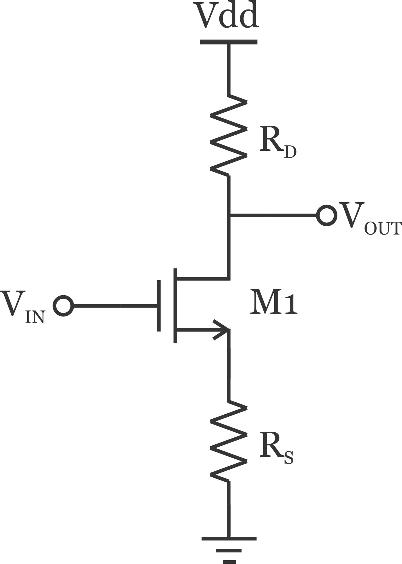
Figure 3. Source degeneration used as a basic linearization technique.
Ignoring the output resistance of the transistor, the transconductance of this circuit is given by:
\[G_m= \frac {g_{m1}}{1+g_{m1}R_S}\]
Equation 2
Assuming that \(g_{m1}R_S \gg 1\), we have \(G_{m1} \simeq \frac {1}{R_S}\), which is independent of the input amplitude. This linearity improvement is achieved at the expense of reducing the gain. Without the degeneration resistor \((R_S=0)\), we would have a transconductance of \(g_{m1}\). If we add the degeneration resistor, the circuit becomes linear; however, the overall transconductance is reduced to that given by Equation 2. (Note that the denominator of this equation is assumed to be much greater than one, hence, the transconductance is decreased.) Therefore, there can be a trade-off between gain and linearity.
Noise-and-Linearity Trade-off
The linearity of a circuit can also trade with its noise performance. This can be simply understood by noting the fact that we have to increase the circuit complexity to make it more linear. The added elements will contribute to the overall noise of the circuit. For example, the degeneration resistor in Figure 3 will act as an additional noise source.
Conclusion
In analog design, we have to consider several aspects of circuit performance such as speed, power consumption, linearity, noise, input/output impedance, stability, and voltage swings. There are usually trade-offs between these parameters, and we cannot improve all of them simultaneously. In this article, we discussed the common trade-offs we face when trying to improve the linearity of a circuit. We saw that circuit linearity usually trades with parameters such as gain, noise, and speed.
Related Content