
Assessing the Effect of Load Capacitance on the Frequency of a Quartz Crystal
Learn how the load capacitance mismatch can “pull” the crystal to oscillate at a different frequency and how we can circumvent this problem.
In the first part of this series, we looked at some of the important metrics that are used to characterize the frequency deviations of quartz crystals.
In this article, we'll discuss another important factor that affects the oscillation frequency: the load capacitance of the crystal. The article also delves into some important specifications, such as pulling curve and trim sensitivity, that is used to characterize the effect of the load capacitance on the oscillation frequency.
Load Capacitance of a Crystal: A Key Factor
Many quartz crystal oscillators, such as Pierce, Colpitts, and Clapp-style topologies, operate the crystal in its inductive region (between fs and fa in the reactance curve shown in Figure 1).
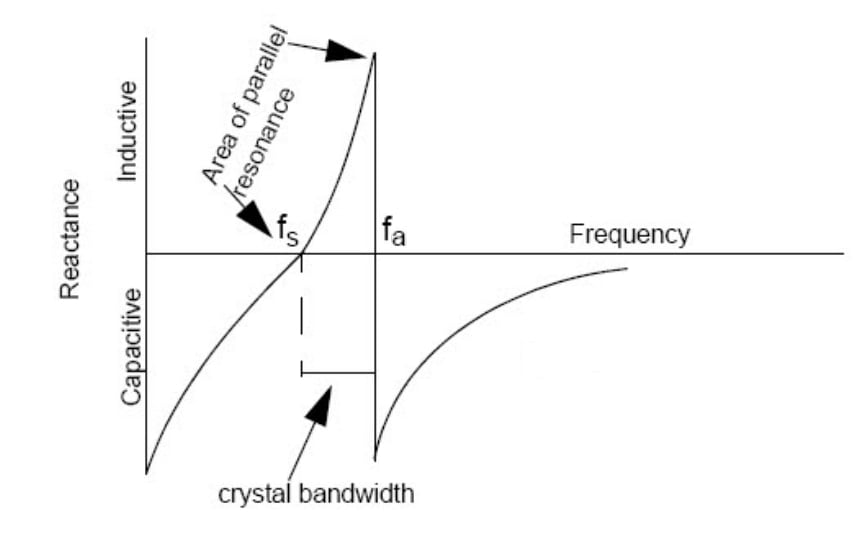
Figure 1. Image courtesy of Cypress.
With these oscillators, the total capacitance “seen” from the crystal terminals is of paramount importance. This capacitance that is created by the oscillator circuit is commonly referred to as the load capacitance of the crystal. How does this load capacitance affect our design? Since the crystal operates between fs and fa, it is effectively acting as an inductor. This effective inductance along with the load capacitance forms an LC tank that determines the oscillation frequency. If the load capacitance is CL and the crystal oscillates at fL, the reactance of the load capacitance is:
\[X_{C_L} = - \frac{1}{2\pi f_LC_L}\]
The crystal will oscillate at a frequency where it exhibits a reactance of \[\frac{1}{2\pi f_LC_L}\].
Hence, a given load capacitance restricts the crystal to oscillate at a specific point between fs and fa. If we change the load capacitance, a different oscillation frequency will be obtained. That’s why the crystal manufacturer gives the crystal frequency at a specific load capacitance.
Matching the Load Capacitance
A common arrangement for connecting a crystal to a microcontroller is shown in Figure 2.
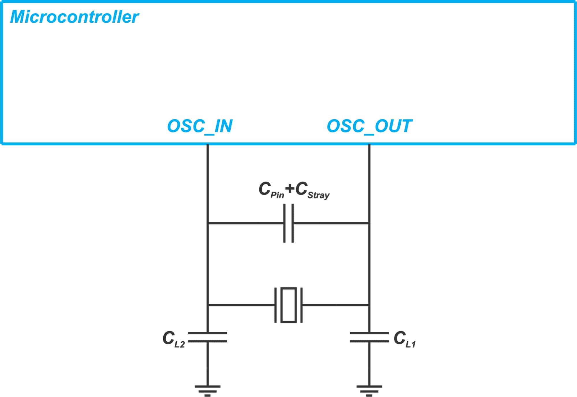
Figure 2.
Here, CPin+CStray models the capacitance of the MCU pins as well as the stray capacitance of the PCB traces connected to the crystal terminals. CPin+CStray is typically in the range from 2 pF to 5 pF. Shorter PCB traces can reduce the stray capacitance.
We also have CL1 and CL2 that is added to match the load capacitance of the board to that specified by the crystal manufacturer. These two capacitors are in series connection through the ground. Hence, the effective load capacitance of the circuit is:
\[C_{Load} = \frac{C_{L1} \times C_{L2}}{C_{L1} + C_{L2}} + C_{Pin} + C_{Stray}\]
This total load capacitance should match the value specified by the crystal manufacturer. If our circuit presents a different load capacitance to the crystal, it will not oscillate at the specified nominal frequency. It will be “pulled” to a slightly different frequency.
The remaining question is, how far the frequency of a given crystal will be pulled as we change the load capacitance?
To answer this question, we first need to derive an equation that gives the oscillation frequency for arbitrary load capacitance.
Oscillation Frequency at an Arbitrary Load
Assume that the crystal is connected to an arbitrary load capacitance CL as shown in Figure 3.
At what frequency the crystal will oscillate?
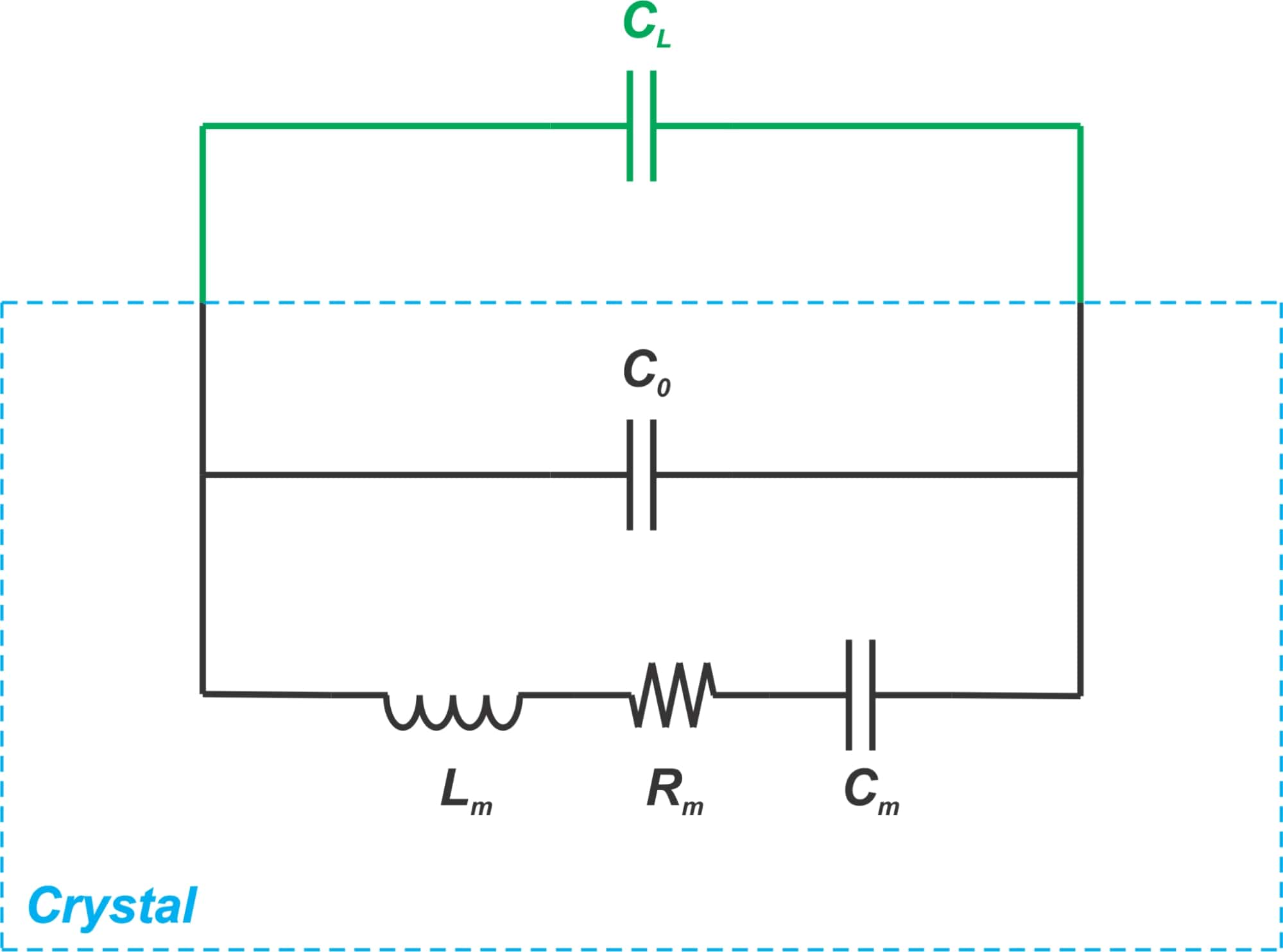
Figure 3.
Ignoring the crystal resistance Rm, the resonance occurs at the frequency where the total admittance of the above network becomes zero:
\[jC_L\omega_L + jC_0\omega_L + \frac{1}{jL_m\omega_L + \frac{1}{jC_m\omega_L}} = 0\]
where ωL = 2πfL and fL denote the oscillation frequency at CL. Using some algebra, we arrive at the following equation:
\[f_L = \frac{1}{2\pi\sqrt{L_mC_m}} \times \sqrt{1 + \frac{C_m}{C_L+C_0}}\]
Equation 1.
It can be shown that the series resonant frequency (fs) of the crystal is given by:
\[f_s = \frac{1}{2\pi\sqrt{L_mC_m}}\]
Hence, Equation 1 simplifies to:
\[f_L = f_s\sqrt{1 + \frac{C_m}{C_L + C_0}}\]
Since Cm≪ C0 + CL, we can use Taylor's theorem to approximate this equation as:
\[f_L = f_s\left(1 + \frac{C_m}{2(C_L + C_0)}\right)\]
Equation 2.
This is an important equation and shows how the crystal oscillation frequency changes with the load capacitance.
Pulling Curve
When the load capacitance of our circuit does not match the nominal value, the crystal will be pulled to oscillate at a slightly different frequency. We need to know how far the frequency of a given crystal will be pulled as we change the load capacitance.
To characterize this, we can rearrange Equation 2 as:
\[\frac{\Delta f}{f_s} = \frac{f_L - f_s}{f_s} = \frac{C_m}{2(C_L + C_0)}\]
To express the frequency variations in ppm, we only need to multiply the result by 106 leading to:
\[\frac{\Delta f}{f_s} = \frac{f_L - f_s}{f_s} = \frac{C_m}{2(C_L + C_0)} \times 10^6 (in~ppm)\]
Equation 3.
The graphical representation of this equation is sometimes referred to as the pulling curve of the crystal. For example, with Cm=20 fF, C0=4.5 pF, we obtain the following pulling curve.
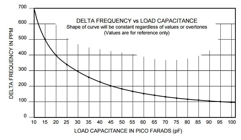
Figure 4. Image courtesy of Ecsxtal.
This curve shows how the crystal frequency changes with the load capacitance. For example, with the above crystal, the oscillation frequency is about +200 ppm higher than fs when a load capacitance of 45 pF is employed.
There are applications where we need to change the crystal frequency by changing its load capacitance. In these applications, we need crystals that can offer a higher “pullability”. The pulling curve allows us to assess the pullability of the crystal. In the example depicted in Figure 4, we observe that the crystal frequency changes from +100 ppm to +700 ppm with respect to fs as the load capacitance changes from 100 pF to 10 pF.
Fine-Tuning the Oscillation Frequency
We saw that the pin and stray capacitances of the design can contribute to the load capacitance and affect the oscillation frequency. Besides, the capacitors connected to the crystal terminals (CL1 and CL2 in Figure 2) have limited tolerances.
We need to take these variations into account to adjust the oscillation frequency. In these cases, we can use additional series and parallel capacitors to modify the load capacitance and pull the crystal back to its desired operating frequency.
An example schematic is shown in Figure 5.
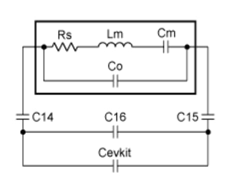
Figure 5. Image courtesy of Maxim Integrated.
Here, Cevkit denotes the IC pin capacitance as well as the stray capacitance from PCB traces. C14 and C15 are the series pulling capacitors and C16 is a parallel pulling capacitor. A series capacitor will raise the oscillation frequency and a parallel capacitor will slow it down.
Some ICs employ an array of internal capacitors to allow the user to fine-tune the load capacitance and meet the frequency tolerance requirements of the application. Figure 6 illustrates this technique employed in MC13224, a ZigBee platform from NXP.
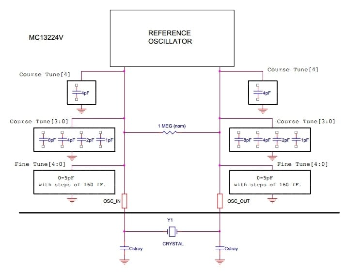
Figure 6. Image courtesy of NXP.
According to the device datasheet, the oscillation frequency can be adjusted to be ±30 ppm from the target frequency overall conditions. On-chip load capacitors can also save the board area. Note that the topologies shown in Figure 5 and 6 assume that the crystal can provide the required pullability.
Trim Sensitivity
As you can see from Figure 4, the slope of the pulling curve reduces as we increase the load capacitance. This indicates that the frequency sensitivity to component tolerances reduces at a higher load capacitance.
To characterize this, we can take the first derivative of the pulling equation (Equation 3) with respect to CL. This gives us the following equation that is commonly referred to as the trim sensitivity:
\[TS = -\frac{C_m}{2(C_L + C_0)^2} \times 10^6 (ppm / pF)\]
For example, with Cm=20 fF, C0=4.5 pF, we obtain the trim sensitivity curve shown in Figure 7.
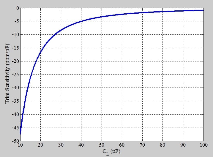
Figure 7.
The above graph shows that at lower load capacitances, the circuit exhibits a higher sensitivity to the value of the load capacitance. In certain designs, such as wearable applications, we might want to use a crystal with lower load capacitance to reduce the power consumption and accelerate the oscillator startup; however, the above curve shows that this can increase the sensitivity of the oscillator to the stray capacitances of the circuit.
It is possible to use the trim sensitivity specification to assess the frequency change caused by a change in the load capacitance. However, one should note that a given trim sensitivity value is only valid within a few picoFarads of the stated load capacitance.
For example, the above graph shows that the trim sensitivity is -5 ppm/pF at CL=40 pF. This trim sensitivity is only valid around CL=40 pF. If the load capacitance changes only slightly, we can multiply the change in the load capacitance by the trim sensitivity value to obtain the frequency variation. For example, if the load capacitance is increased from 40 pF to 41 pF, we expect the frequency to change by about -5 ppm. However, if the load capacitance changes by several pico-Farads, we cannot use the trim sensitivity value to find the frequency variation.
To see a complete list of my articles, please visit this page.


