Basics of Phase Truncation in Direct Digital Synthesizers
This article will discuss phase truncation in direct digital synthesizers.
This article will discuss phase truncation in direct digital synthesizers.
In one of our previous articles, Everything You Need to Know About Direct Digital Synthesis, we saw that a direct digital synthesizer (DDS) uses an accumulator along with a lookup table (LUT) to produce digitized samples of a sinusoid. The accumulator generates the phase argument of the output sinusoid and the LUT performs phase-to-amplitude conversion.
In this article, we’ll discuss that, in practice, the output of the phase accumulator should be truncated before being passed on to the LUT. We’ll also briefly review the consequences of this phase truncation for the output spectral purity of the DDS.
Basic Operation of a DDS
Assume that we want to generate a digitized sinusoid. Since a sinusoid is a periodic signal, we can store samples of one period in a memory and use these samples to generate as many cycles as we want. Figure 1 shows an example where 16 samples of one period of the analog sinusoid are taken. Using these samples, we can generate the desired periodic signal. The time-domain sampling shown in Figure 1 is, in fact, equivalent to quantizing the phase argument of a sinusoid.
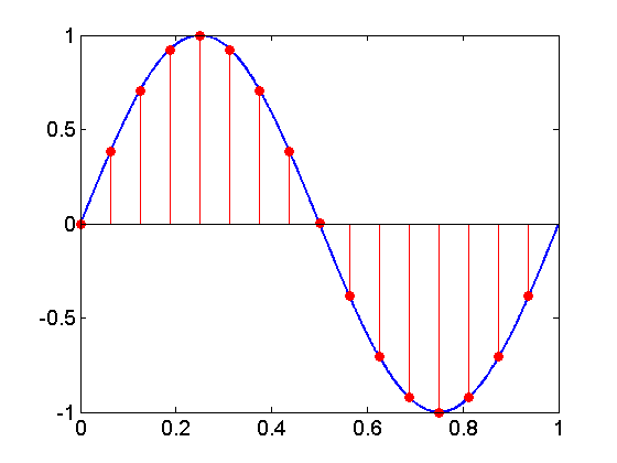
Figure 1
In this example, 16 different levels are used to quantize the range from 0 to $$2 \pi$$.
This phase quantization is shown in Figure 2 using the trigonometric unit circle.
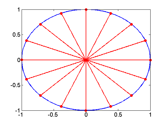
Figure 2
Now, imagine that we store these 16 samples in a ROM and use a clock signal with period $$T_{clk}$$ to read the samples sequentially. Each sample will last for one $$T_{clk}$$ and, hence, it will take $$16 \times T_{clk}$$ to produce one period of the sinusoid. As you can see, the frequency of the produced sine will be $$f_{out}=\tfrac{1}{16 \times T_{clk}}$$.
Note that, for a given clock frequency, we can change the output frequency by changing the number of utilized samples. For example, if we sequentially read only eight equally-spaced samples out of the available 16 samples of Figure 1 (every other sample), the output frequency will increase to $$f_{out}=\tfrac{1}{8 \times T_{clk}}$$. In this case, we’re reading every other sample of Figure 1. In other words, to produce $$f_{out}=\tfrac{1}{16 \times T_{clk}}$$, we are using a phase increment of $$\tfrac{2 \pi}{16}$$ between the discrete levels representing the range from 0 to $$2 \pi$$; however, for $$f_{out}=\tfrac{1}{8 \times T_{clk}}$$, the phase increment between the discrete levels is increased to $$\tfrac{2 \pi}{8}$$.
This is the basic idea of a DDS: We store a relatively large number of samples in a ROM and sequentially read the samples with an appropriate phase increment to produce different frequencies of the stored waveform. Based on this discussion, we obtain the basic block diagram of a DDS as shown in Figure 3.
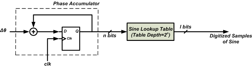
Figure 3
As you can see, $$2^n$$ samples of the sine are stored in a lookup table (LUT). The address input of the LUT is connected to a block called “Phase Accumulator”. The “Phase Accumulator” is simply an adder followed by a set of n registers. As shown in the figure, the registered output is used as an input to the adder. Hence, with each clock edge, the value stored in the set of registers will increase by the value of $$\Delta \theta$$. In this way, we can control the number of samples that are read from the LUT and we will be able to control the frequency of the output sinusoid. Extending the simple example discussed above, we can find the output frequency of the DDS as
$$f_{out}=\frac{f_{clk}}{2^n}\times \Delta \theta$$
The Frequency Resolution of a DDS
Equation 1 shows that the output frequency of a DDS is an integer multiple of $$\tfrac{f_{clk}}{2^n}$$. Substituting the phase increment with its minimum possible value, i.e. $$\Delta \theta =1$$, we obtain the frequency resolution of the DDS as
$$\Delta f=\frac{f_{clk}}{2^n}$$
Equation 2
Equation 2 shows that, for a given $$f_{clk}$$, the frequency resolution can be improved only by increasing n. That’s why a DDS with a large accumulator is desired. For example, utilizing an accumulator with n=48, Analog Devices AD9912 can provide a frequency resolution of approximately 3.6 Hz while operating with $$f_{clk}=1GHz$$.
Phase Truncation
A large accumulator can yield an arbitrarily small frequency tuning resolution; however, with the structure shown in Figure 3, a large accumulator mandates use of an impractically large LUT. To circumvent this problem, we generally truncate the output of the accumulator. This is shown in Figure 4.
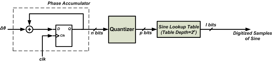
Figure 4
The “Quantizer” accepts the n-bit output of the accumulator and applies only the p most significant bits (MSBs) to the LUT. You may wonder why we used a large accumulator in the first place if we were going to discard some of the LSBs and apply only the p MSBs to the address input of the LUT?
To have a better insight, let’s add two more bits to the phase quantization of Figure 2 but discard these two additional bits when going to the LUT. The phase quantization of our six-bit accumulator is shown in Figure 5. In this figure, the red circles represent the phase quantization levels achieved by the four MSBs of the accumulator, hence, the phase difference between two adjacent red circles is $$\tfrac{2 \pi}{16}$$.
As you can see, the black dots divide every arc between two successive red circles into four discrete levels. These black dots correspond to the two LSBs of the accumulator. The phase difference between two adjacent black dots is $$\tfrac{2 \pi }{64}$$. Now, assume that the accumulator is reset to zero and $$\Delta \theta =3_{10}$$ in Figure 4. The discrete levels successively obtained from the accumulator output will be as shown by the triangles of Figure 5.
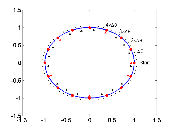
Figure 5
Note that the triangles are in black when they correspond to a black dot and are in red when they coincide with a red circle. With an accumulator reset to zero, the starting point will be as shown in the figure.
With the next clock edge, the accumulator output will be three. As you can see, this falls short of the first red circle. Therefore, the value that will be passed on to the LUT will correspond to the first sample stored in the LUT (just like when we were in the “start” point). Hence, the truncation process leads to a phase error of $$3 \times \tfrac{2 \pi}{64}$$ at this point. This phase error will lead to an amplitude error because the LUT will output the sample corresponding to the “start” point.
With the next clock edge, the accumulator will increase by another three and we will reach the point specified by $$2 \times \Delta \theta$$. In this case, the truncated phase value will point to the second sample stored in the memory. This time, the phase error will be $$2 \times \tfrac{2 \pi}{64}$$.
This process will go on and, after two more additions, we’ll reach the point $$4 \times \Delta \theta$$. The triangle of this point is shown in red because it corresponds to a discrete level obtained from the four MSBs of the accumulator. At this point, the truncation won’t lead to a phase error.
This example emphasizes three points: First, a large accumulator increases the frequency tuning resolution no matter whether we perform phase truncation or not. In fact, for a given $$f_{clk}$$ and $$\Delta \theta$$, a larger accumulator will need more time to overflow and will yield a higher resolution frequency.
Second, since we’re truncating the accumulator output, the phase information passed on to the LUT may experience some error. However, the maximum of this error can be limited by the number of the accumulator bits that are kept after the truncation. This limited phase error can be envisioned as a time base jitter. As we increase p in Figure 4, the depth of the LUT will increase but the maximum error due to the phase truncation will reduce.
To summarize these two points, we are increasing the frequency resolution of the DDS at the cost of some phase error. This is an interesting idea mainly because we can limit the maximum value of the phase error by passing sufficient number of the accumulator bits to the LUT.
The third point, it can be verified that the phase error arising from truncation is periodic. In the discussed example, we saw that the phase error of the first four additions were $$3 \times \tfrac{2 \pi}{64}$$, $$2 \times \tfrac{2 \pi}{64}$$, $$1 \times \tfrac{2 \pi}{64}$$ and zero. You can verify that this sequence of error terms will be repeated for the next additions too.
Phase Truncation Spurs
The periodic error from phase truncation leads to a periodic error in the amplitude of the DDS output signal. In the output spectrum, the periodic amplitude error generates undesired frequency components called phase truncation spurs. The magnitude and distribution of the phase truncation spurs depend on three parameters:
- The size of the accumulator (n)
- The number of the accumulator bits that are passed on to the LUT (p)
- The value of the phase increments ( $$\Delta \theta $$)
Analyzing the magnitude and especially the distribution of the spurs is quite complicated. You can find a summary of the analysis in Section 10.3.3 of this book. Here, we will only review the result of the magnitude analysis. According to this analysis, the maximum magnitude of a phase truncation spur is about 6.02p decibels below the magnitude of the desired output. For example, with p=8, the maximum spur will be about 48 dB below the desired output of the DDS. This is shown in Figure 6.
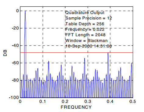
Figure 6. The DDS output spectrum with $$f_{out}=0.022$$Hz, n=p=8, and l=12. Image courtesy of Xilinx.
It’s worth to note that two types of quantizations can be recognized in a basic DDS structure: 1- Phase quantization which was discussed above and 2- The amplitude quantization which corresponds to the number of bits utilized to represent the samples of the sinusoid in the LUT. For example, by increasing l in Figure 4, we can get a better approximation of the sinusoid samples.
Interestingly, the maximum spur level shown in Figure 6 depends on the depth of the LUT, i.e. p, rather than its width (l). For example, if we use l=16 bits to represent each sample of a sinusoid and keep the other parameters of the simulation shown in Figure 6 unaltered, again the maximum spur level will be about 48 dB below the desired output of the DDS. This is shown in Figure 7.
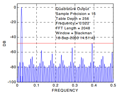
Figure 7. The DDS output spectrum with $$f_{out}=0.022$$Hz, n=p=8, and l=16. Image courtesy of Xilinx.
Summary
A large accumulator can yield an arbitrarily small frequency tuning resolution; however, this will mandate use of an impractically large LUT. To circumvent this problem, we generally truncate the output of the accumulator. In this case, we are increasing the frequency resolution of the DDS at the cost of some phase error. This is an interesting idea mainly because we can limit the maximum value of the phase error by passing sufficient number of the accumulator bits to the LUT.
The error from phase truncation is periodic and leads to undesired frequency components called phase truncation spurs. The maximum magnitude of a phase truncation spur is about 6.02p decibels below the magnitude of the desired output. For example, with p=8, the maximum spur magnitude will be about 48 dB below the desired output of the DDS.
References
- “Integrated Circuit Design for High-Speed Frequency Synthesis” by John Rogers.
- “Digital Waveform Generation” by Pete Symons.
- Xilinx LogiCORE IP DDS Compiler v4.0
- Direct Digital Synthesis Theory & Applications
- A Technical Tutorial on Digital Signal Synthesis
To see a complete list of my articles, please visit this page.