 Facebook
 Google
 GitHub
 Linkedin
BJTs after Biasing: Analyzing BJTs with a Small-Signal Model
This article presents two circuits that can be used to analyze the small-signal behavior of a bipolar junction transistor.
This article presents two circuits that can be used to analyze the small-signal behavior of a bipolar junction transistor.
Supporting Information
We frequently use BJTs as a straightforward electrical switch (as described in my previous article on rapid analysis of BJT switch/driver circuits). These applications focus on the “large-signal” conditions of the transistor, meaning the DC currents and voltages that determine the transistor’s operating mode and the total current flowing into or out of its base, collector, and emitter.
BJTs are also capable of amplifying small-amplitude signals, and amplifier applications such as these lead us into the “small-signal” realm. This realm does not replace the large-signal conditions; rather, small-signal operation is superimposed on large-signal operation. We use large-signal conditions to bias the transistor, and the biasing conditions imposed by a given circuit influence the BJT’s small-signal behavior.
Small-Signal Models
After the BJT has been biased, we can focus on small-signal operation, and small-signal analysis is easier when we replace the BJT with simpler circuit elements that produce functionality equivalent to that of the transistor. Just remember that these models are relevant only to small-signal operation, and furthermore, you can’t use the models until you have established the large-signal bias conditions.
The Hybrid-π Model
The first small-signal model that we’ll discuss is called the hybrid-π model, and it looks like this (for an NPN transistor):
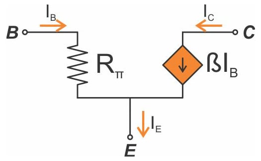
As you can see, it has three terminals corresponding to the BJT’s base, collector, and emitter. The current flowing into the base is determined by the base-to-emitter voltage (VBE) and Rπ, and the collector current is generated by a current-controlled current source. Just as with a large-signal NPN, the collector current flows into the collector, the base current flows into the base, and the emitter current flows out of the emitter and is the sum of the base current and the collector current.
The collector current is equal to β times IB, which is not surprising. IB is determined by VBE and Rπ, and this is where the biasing conditions come into play:
$$R_{\pi}=\frac{\beta}{g_m}$$
$$g_m=transconductance=\frac{I_{C_{BIAS}}}{V_t}$$
So we need IB to determine IC, and we need Rπ to determine IB, and we need gm to determine Rπ, and we need ICBIAS (i.e., the large-signal collector current) to determine gm.
It is possible to reformulate the hybrid-π model so that you calculate directly from VBE to IC. If you replace β with gmRπ, you have IC = IBgmRπ = gmVBE.
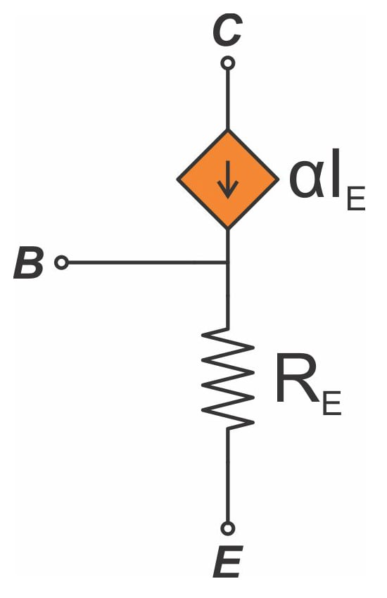
The T Model
In some cases you might prefer to use the following alternative to the hybrid-π model:
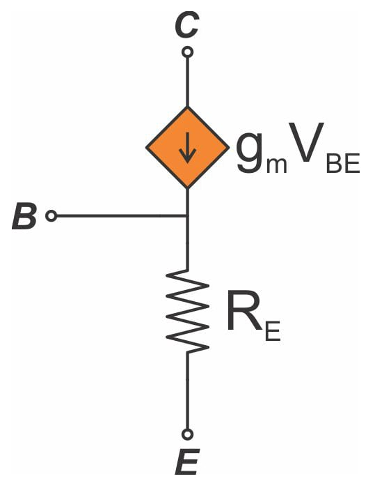
This is called the T model. It looks quite different from the hybrid-π model, but they are both valid in all cases and will produce equal results (as long as you get the math right). With the T model, you again need to know the large-signal collector current (to calculate gm), because the resistance RE is calculated as follows:
$$R_E=\frac{\alpha}{g_m}$$
You can use the following formula to calculate the parameter α:
$$\alpha=\frac{\beta}{\beta+1} $$
As with the hybrid-π model, the T model can use either a voltage or a current as the variable that controls the current source. In the T model, the current source’s expression is either gmVBE (as shown above) or αIE:
Using the Models
The BJT small-signal models are drop-in replacements for the BJT symbol in a circuit diagram. Once you have determined the bias conditions, you remove the BJT, insert the small-signal model, and connect the previous base, collector, and emitter nodes to the model’s base, collector, and emitter terminals.
The next step is not so obvious: you need to replace each DC voltage source with a short circuit and each DC current source with an open circuit, because this corresponds to their behavior in the context of small-signal operation. Note that a “voltage rail” (e.g., VCC, VDD) that appears in the schematic as simply a supply voltage becomes a ground connection, because the rail is actually a shorthand way of drawing a normal voltage source that has one terminal connected to ground.
At this point you have converted the circuit from large signal to small signal, and you’re ready to proceed with standard circuit-analysis procedures.
Accounting for the Early Effect
I have an article that serves as an introduction to the Early effect if you'd like a more thorough explanation. To make a long story short, however, the Early effect refers to a phenomenon that occurs inside a BJT and causes the active-mode collector current to be affected by the collector voltage. More specifically, an increase in the collector-to-emitter voltage results in an increase in the collector current.
If you ponder the small-signal models shown above, you can see that they don’t incorporate the Early effect: the only small-signal variable that affects the collector current is the base current, the emitter current, or the base-to-emitter voltage. If we want the small-signal models to be more accurate, we need to account for the Early effect.
Fortunately, this is easily done. All we need is a resistor connected between the collector and the emitter.
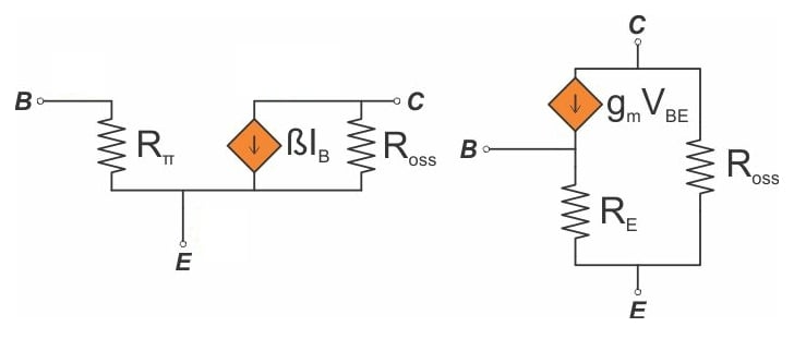
This resistor represents the small-signal output resistance, which is calculated as follows:
$$R_{O_{SS}}=\frac{V_A+V{_{CE_{BIAS}}}}{I_{C_{BIAS}}}$$
The Early voltage (VA) will often be significantly larger than the collector-to-emitter voltage, so you can simplify this as follows:
$$R_{O_{SS}}=\frac{V_A}{I_{C_{BIAS}}}$$
The addition of this resistor makes intuitive sense: the Early effect tells us that a higher collector-to-emitter voltage will result in higher collector current, and by adding this resistor we are opening an additional current path between collector and emitter that is directly influenced by the collector-to-emitter voltage.
Conclusion
We briefly covered the concept of separating large-signal conditions from small-signal behavior in the context of amplifier analysis, and we looked at two circuit structures (the hybrid-π model and the T model) that correspond to the small-signal functionality of a bipolar junction transistor. After a quick explanation of how to incorporate these models into BJT circuit analysis, we discussed improved versions that use a collector-to-emitter resistor to account for the Early effect.


Articles are simple superb. Easy to understand and have been very helpful for a beginner like me. Please keep writing.
Very informative, but the majority of BJT data sheets no longer provide many of these parameters. What to do then?