Facebook
 Google
 GitHub
 Linkedin
Clock Signals in FPGA Design: Data Path Maximal Clock Rates and the Xilinx PERIOD Timing Constraint
This article will discuss the Xilinx Period timing constraint that allows us to describe the characteristics of the clock signal that will be used with an FPGA design.
This article will discuss the Xilinx Period timing constraint that allows us to describe the characteristics of the clock signal that will be used with an FPGA design.
This article will first discuss the different delays that are observed when propagating data in a typical path of a digital system. After finding the equation for the maximal clock rate of this typical data path, we’ll discuss the Xilinx Period timing constraint. This fundamental timing constraint allows us to describe the characteristics of the clock signal that will be used with an FPGA design.
Typical Paths in a Digital System
In an FPGA design, we generally have combinational circuits with intermediate layers of registers. Figure 1 below shows a simple example of this concept.
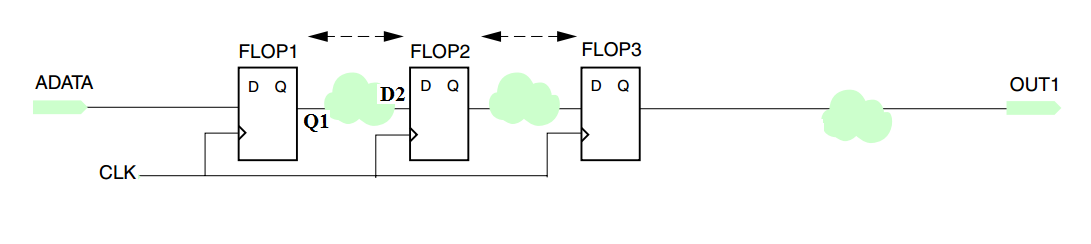
Figure 1. A basic representation of combinational circuits with layers of registers in an FPGA design
In this figure, the clouds represent combinational circuits.
How to Calculate Maximal Clock Rate
Let’s examine the maximal clock rate that can be applied to the block diagram of Figure 1. To do this, we’ll examine the different delays that are introduced to the data propagating from input, ADATA, to the input of the second flip-flop, D2.
As shown in Figure 2, at the rising edge of the clock, a particular sample from the input data, ADATA1, is taken by the first flip-flop, FLOP1. A flip-flop cannot update its output immediately after the clock edge. Due to this delay, which is called the clock-to-Q delay, the output of FLOP1 will change at $$t_1$$ as shown in Figure 2. Hence, $$t_1 = t_0 +\Delta T_{clk-to-Q}$$.
Note that the parts of the waveforms that correspond to samples taken before ADATA1 are shown in red in Figure 2.
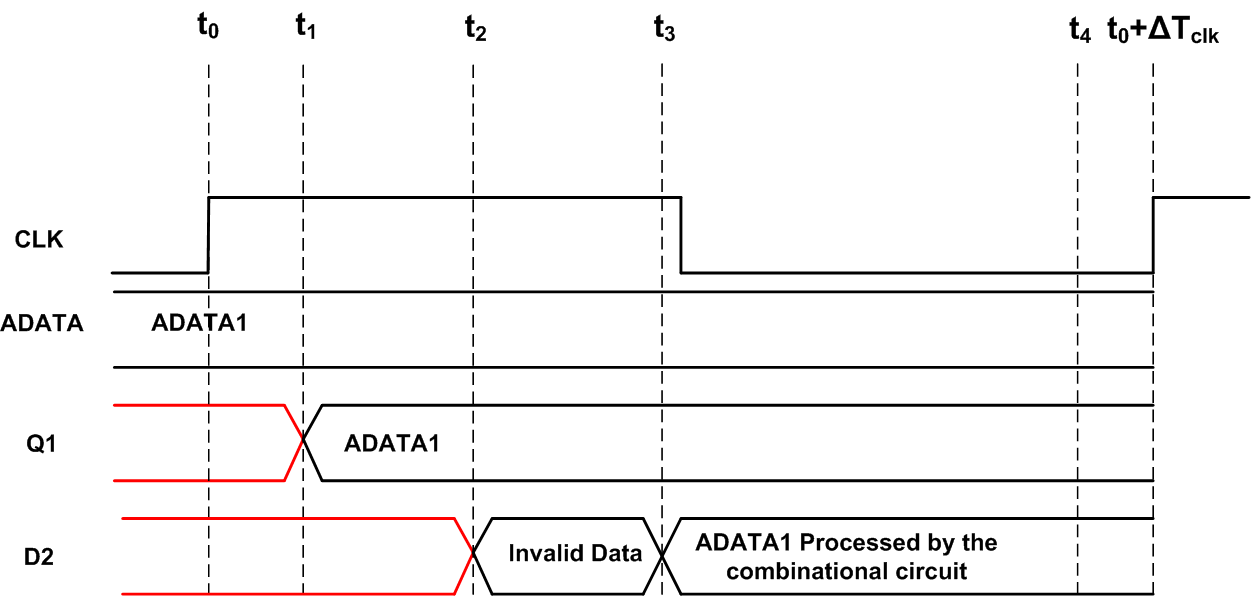
Figure 2
Then, ADATA1 will be processed by the combinational circuit between FLOP1 and FLOP2. Assume that, based on the value of the input, the delay of this combinational circuit can vary between a minimum and a maximum value that are $$\Delta T_{comb, \; min}$$ and $$\Delta T_{comb, \; max}$$, respectively. When the circuit responds with its minimum delay, we obtain the data at $$t_2 = t_0 +\Delta T_{clk-to-Q} + \Delta T_{comb, \; min}$$. When the circuit exhibits its maximum delay, we have the processed data at $$t_3 = t_0 + \Delta T_{clk-to-Q} + \Delta T_{comb, \; max}$$. Hence, to make sure that the data is valid for any input, we should wait until $$t_3$$ as shown in the figure.
Synchronous Element Setup Time
In addition to the delays that we’ve discussed so far, there is another important timing issue called the synchronous element setup time ($$\Delta T_{setup}$$). According to the setup time constraint, a synchronous element can successfully take a sample from its input only if the input signal is stable at least $$\Delta T_{setup}$$ before the sampling clock edge.
In Figure 1, Flop2 will sample the data processed by the combinational circuit. Therefore, we should take the setup time constraint of FLOP2 into account.
With the example waveforms shown in Figure 2, the sampling edge of FLOP2 is at $$t_0 + \Delta T_{clk}$$ where $$\Delta T_{clk}$$ is the clock period. Therefore, the data processed by the combinational circuit must be ready at $$t_4$$ which is $$\Delta T_{setup}$$ before $$t_0 + \Delta T_{clk}$$, i.e. $$t_4 = t_0 + \Delta T_{clk} - \Delta T_{setup}$$. Hence, $$t_3 \leq t_4$$ must be satisfied which gives
$$ t_0 + \Delta T_{clk-to-Q} + \Delta T_{comb, \; max} \leq t_0 + \Delta T_{clk} - \Delta T_{setup} $$
From this, we know the minimum clock period will be $$\Delta T_{clk, \; min} = \Delta T_{clk-to-Q} + \Delta T_{comb, \; max} + \Delta T_{setup}$$.
This gives the maximum clock frequency as
$$f_{clk, \; max} = \frac{1}{\Delta T_{clk-to-Q} + \Delta T_{comb, \; max} + \Delta T_{setup}}$$
Equation 1
With a clock frequency higher than $$f_{clk, \; max}$$, the correct operation of the circuit is not guaranteed. Note that we’ve only analyzed the data propagation from the input ADATA to the input of the second flip-flop D2. A similar analysis can be applied to the rest of the data path and, then, we can choose a maximum clock frequency that satisfies the timing requirements of all parts of the data path.
If we need to operate this circuit at a clock frequency higher than $$f_{clk, \; max}$$, we can examine adding more layers of registers. This will reduce $$T_{comb, \; max}$$ and increase $$f_{clk, \; max}$$ according to Equation 1.
Note that clock skew can also affect the maximal clock rate that we can apply to a circuit. The clock skew is a phenomenon in which the same sourced clock signal arrives at different components at different times. You can find some details about the clock skew phenomenon and methods of de-skewing the clock signals in my article on clock resources of FPGAs. The above discussion has not included the effect of clock skew in the maximal clock rate equation. Refer to Chapter 16 of RTL Hardware Design Using VHDL: Coding for Efficiency, Portability, and Scalability for more information.
There remains one important question: how do we take all these timing requirements into account when we synthesize the VHDL code of the block diagram in Figure 1? We may assume a clock frequency based on the system level requirements but how do we convey these pieces of information to the synthesis tool? This is achieved by the timing and synthesis constraints that an FPGA design tool supports. As the name suggests, a constraint forces the design tool to satisfy a particular requirement. This particular requirement may or may not be satisfied if we don’t specify the corresponding constraint. In other words, a constraint directs the software toward implementing the HDL code in a particular way.
Note that there are many constraints but, in this article, we’ll focus on a fundamental timing and synthesis constraint for the Xilinx tools which is called the PERIOD constraint.
The PERIOD Constraint
The Xilinx PERIOD constraint defines the period of the clock that will be used to operate the implemented HDL code. For example, assume that you’ve written the VHDL code for the block diagram of Figure 1. Then, you have a port called CLK in your entity. If you don’t specify the PERIOD constraint for this clock, the synthesis software doesn’t actually know the frequency of the clock that you’ll connect to the CLK port. The software will synthesize your code based on some default settings even if you don’t have the PERIOD constraint. However, when you connect your design to a clock with a given frequency, your circuit may or may not work as expected.
When you specify the PERIOD constraint for CLK in Figure 1, the synthesis software performs a timing analysis similar to the one we manually did in the previous section. It finds all the synchronous elements that are connected to CLK and, then, examines the timing requirements of all the combinational circuits that are between two synchronous elements connected to CLK. If your design can reliably work at the specified clock frequency, the software will report that timing requirements were met otherwise it will give the paths that have timing problem.
Note that PERIOD is a global constraint and will be applied to all the paths that are between two synchronous elements connected to CLK.
The Syntax of the PERIOD Constraint
Assume that we’ll operate the block diagram of Figure 1 at a clock rate of 50 MHz. To specify the PERIOD constraint for the CLK port, we first need to add a “user defined constraint file (.ucf)” to our Xilinx project as will be explained in the next section. Then, we can include the following line in our ucf file to specify the clock period:
NET CLK PERIOD = 20 ns;Here, “NET” and “PERIOD” are keywords and CLK is the name of our clock signal. Another syntax to specify this constraint is by using the TIMESPEC keyword:
NET CLK TNM = SYSCLK;
TIMESPEC TS_SYSCLK = PERIOD SYSCLK 20;
The first line uses the keyword TNM, which stands for “timing name”, to create a user-defined group with the name SYSCLK. The second line uses the keyword TIMESPEC to define the timing specifications on the created group. Note that after the keyword TIMESPEC, we have an arbitrary TIMESPEC name that must start with “TS”. Besides, note that the default unit for time is nanoseconds. Xilinx recommends using the second syntax to specify a PERIOD constraint. However, this syntax may seem to be a little bit confusing at first. To become more comfortable with the syntax of both of these methods, apply your knowledge to the following examples:
NET clk20MHz PERIOD = 50;
NET clk50mhz TNM = registers_50mhz ;
TIMESPEC TS01 = PERIOD registers_50mhz 20;
With the period constraint, we can also specify the initial edge, the duty cycle, and the jitter of the utilized clock. An example is given below
TIMESPEC TS_master = PERIOD “master_clk” 50 HIGH 30 INPUT_JITTER 50 ps;This defines a clock period of 50 nanoseconds, with an initial 30 nanosecond high time, and INPUT_JITTER at 50 ps. Note that the HIGH or LOW keyword can be used to indicate whether the first pulse in the period is high or low. Besides, note that we can enclose the TIMESPEC and the NET names in double quotes (see page 35 of the Xilinx Constraint Guide and this Answer Record).
A PERIOD Constraint Example
In a previous article, we discussed the VHDL code for a basic binary division algorithm. Now, we will use a PERIOD constraint to specify the clock frequency of our division algorithm. First, we need to add a User-defined Constraint File (.ucf) to our project. In the ISE software, click on “New Source” and choose “Implementation Constraints File” as the source file type. This is shown in Figure 3 below. Name this new source file “My_Constraints.ucf” and go on with the rest of the “New Source Wizard”.
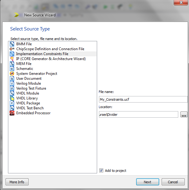
Figure 3
Copy the following lines to your ucf file:
NET "clk" LOC = "p85";

NET "clk" TNM_NET = clk;
TIMESPEC TS_clk = PERIOD "clk" 300 MHz HIGH 50%;
Here, clk is the name of the clock signal used in our division algorithm. The first line specifies that the clk port of the divider entity will be connected to the P85 pin of the FPGA (We’ve used spartan 6 xc6slx9 with TQG144 package for this project.) The next two lines create a user-defined group with the name clk and uses the keyword TIMESPEC to define the timing specifications on the created group. The clock will be a 300-MHz signal with 50% duty cycle. Note that, with the TIMESPEC, you can specify the clock frequency rather than the clock period as was used in the examples of the previous section. Besides, this example specifies the duty cycle as a percentage (50%).
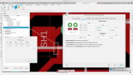
Now, implement the design and choose “Post-PAR Static Timing Report” from the “Design Summary” to see if the timing requirements were met or not. At the end of the report, you’ll see the “Timing summary” as shown in Figure 4.
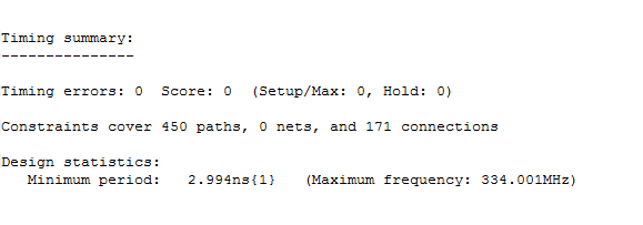
Figure 4
As you can see, there are no timing errors and the maximum frequency of the design is about 334 MHz.
As another experiment, let’s increase the clock frequency to 350 MHz in the ucf file and examine the “Post-PAR Static Timing Report” again. In this case, the “Timing summary” will be as shown in Figure 5.
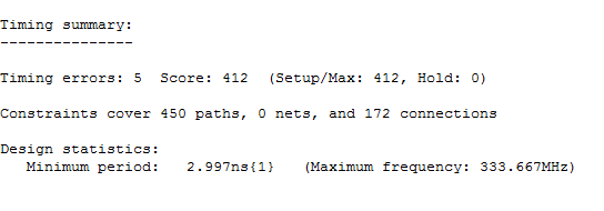
Figure 5
Now, there are timing errors and the maximum clock frequency is lower than our desired frequency. From the timing report we can find out the path that has unacceptable delays and, then, we can try to improve the timing of our design by applying different techniques. You can find some references to these techniques here.
Summary
- The minimum clock period of a digital design is determined by several delay terms such as the flip-flop clock-to-Q delay, setup time delay, and the maximum delay of the combinational circuit between layers of registers.
- We can use the Xilinx PERIOD constraint to specify the characteristics of the clock that will be used to operate the implemented HDL code.
- A constraint directs the FPGA design software toward implementing the HDL code in a particular way.
- With the period constraint, we can specify the period, initial edge, duty cycle, and jitter of the utilized clock.
To see a complete list of my articles, please visit this page.
Related Content