 Facebook
 Google
 GitHub
 Linkedin
Clock Signal Management: Clock Resources of FPGAs
This article will review the common FPGA resources that allow us to efficiently generate and distribute clock signals throughout a system.
This article will review the common FPGA resources that allow us to efficiently generate and distribute clock signals throughout a system.
There are many circumstances in which we need to generate new clock signals and efficiently distribute them throughout a system. Modern FPGAs have dedicated clock management blocks that allow us to perform these two tasks.
In this article, we’ll first briefly review the issues of efficient clock distribution and new clock generation. Then, we’ll see that these two design requirements can be easily handled by the clock management blocks of modern FPGAs.
Efficient Clock Distribution
Even in a small digital design, the clock signals may be distributed to hundreds of clocked elements throughout the system. These high-fanout clock signals are responsible for synchronizing different subsystems or components of the system. That’s why we need to pay careful attention to the delay introduced by different paths of the clock network.
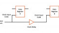
As an example, consider distributing a clock signal from node A to nodes B and C as shown in Figure 1 below. In this figure, the clock signal enters the FPGA and goes through a buffer (shown as a triangle in the figure) and then reaches a register at node B. This path has an inherent delay which is shown by $$\Delta b$$ in the waveforms. To distribute the clock from A to C, we could have used a PCB trace without going through the FPGA but, in the figure, the clock distributed in the FPGA is used for the “Other Device on Board”. The delay of this path is represented by $$\Delta c$$. Since $$\Delta b$$ and $$\Delta c$$ are not equal in general, the register at node B and the device at node C will see slightly different clocks; this fixed time offset between identical clocks that are supposed to have aligned edges is called clock skew. We can see, then, that one serious problem in digital design is distributing high-fanout clock signals across a system with the minimum possible clock skew.
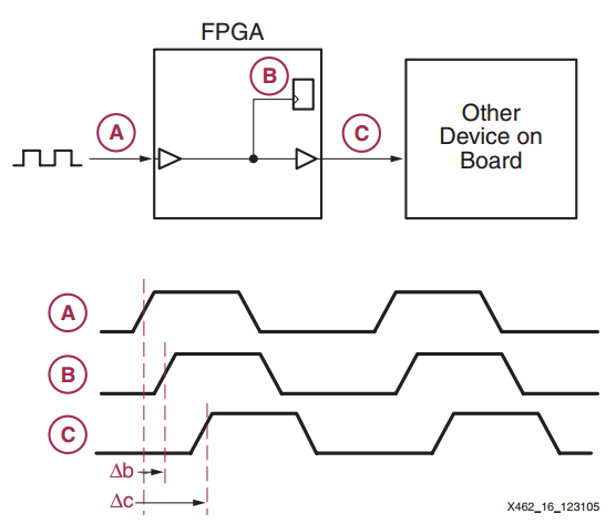
Figure 1. The delay in distributing the clock signal. Image courtesy of Xilinx.
Generating New Clock Signals
A desired feature of an FPGA can be the ability to modify a given clock signal to generate new clocks based on the requirements of the system. For example, assume you’ve designed a board with an FPGA. Suppose that a 50 MHz clock is sufficient for the board but, in the FPGA, you need a 200 MHz clock to perform a particular algorithm. If you could somehow generate a 200 MHz clock from the 50 MHz clock on the board, you could avoid using two different clock sources in your system, and you also would not have to operate the board at a higher-than-necessary frequency. We can identify another application of clock synthesis if we recall that some digital signal processing (DSP) applications are multirate and require different clock frequencies in different parts of the algorithm.
Now, let’s look at the clock-related resources of FPGAs that allow us to generate a new clock signal and distribute it across the system.
Clock Management Resources of FPGAs
Today’s FPGAs incorporate powerful clock management blocks to facilitate the design process and reduce costs. We’ll refer to these embedded clock management blocks as CMBs. Different vendors use different terms to refer to their CMBs. For example, Xilinx uses clock management tile (CMT) or digital clock manager (DCM), Intel uses the well-known term phase-locked loop (PLL), and Microsemi uses clock conditioning circuitry.
The CMBs can generate new clock signals by performing clock multiplication and division. They may be able to apply a programmable phase shift to a generated clock or even adjust the duty cycle of a clock. CMBs can de-skew not only the clock signals distributed within the FPGA but also the clocks distributed out of the FPGA to other devices on the board (such as the clock going to node C in Figure 1).
One application for the programmable phase shift feature is synchronizing the clock signal with input data. When we’re working with digital signals, we have to sample the signal at moments when the data is stable (after the last data transition and before the next transition). That’s why some FPGAs provide a dynamic mechanism for fine phase shift adjustment of the generated clock. For example, the CMBs of the Xilinx Virtex II Pro can apply a phase shift of 1/256th of the clock period. Without this phase shift capability, the clock may not fall at the center of the data eye.
A CMB with the duty cycle adjustment feature can be helpful in applications that need a clock signal with 50% duty cycle. Examples are high-speed communications such as LVDS and dual data rate (DDR) interfaces. If the clock duty cycle is not 50%, we can use the duty cycle correction feature of a CMB to reshape the clock signal to have a 50% duty cycle.
To obtain these features, FPGAs use CMBs based on a phase-locked loop (PLL) or a delay-locked loop (DLL). In addition to the PLLs and DLLs, there’s another very important group of clock-related FPGA resources: the dedicated buffers and routes for distributing the clock signals in the FPGA. These dedicated buffers and routes enable us to have a low-skew clock network.
In the rest of the article, we’ll first review the basic concepts of using a PLL/DLL to implement a CMB. Then, we’ll look at the low-skew clock network employed by the Intel FPGAs.
DLL-Based Clock De-skew
Figure 2 shows the basic block diagram of a DLL used to compensate for clock distribution delay.
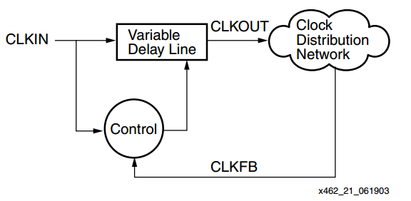
Figure 2. Block diagram showing the use of a DLL to compensate for clock skew. Image courtesy of Xilinx.
In this figure, CLKIN is the input clock that we intend to distribute through the “Clock Distribution Network”. As the name suggests, the “Variable Delay Line” block introduces an adjustable delay to CLKIN and produces CLKOUT. The amount of delay is determined by the “Control” logic. The “Control” block monitors its inputs and varies the delay so that the rising edges of the two inputs, CLKIN and CLKFB, are aligned. In this way, the circuit compensates for the delay in the clock distribution network, and theoretically we can de-skew the clock distribution.
Note that the “Variable Delay Line” cannot apply a negative delay to CLKIN to compensate for the inherent delay of the “Clock Distribution Network”. So, how can the block diagram of Figure 2 eliminate the clock skew? The key point is that the clock signal CLKIN is periodic. To clarify this, let’s consider the clock skew example of Figure 1. The path from A to B has a delay of $$\Delta b$$, therefore, we need to apply a delay of $$- \Delta b$$ (i.e., a negative delay) to the clock at node A and then distribute it through the path with delay $$\Delta b$$. How can we circumvent the problem of creating a negative delay? Remember that the clock signal is a periodic waveform. Assume the period is $$T$$. We know that a periodic function $$f(t)$$ with period $$T$$ satisfies
$$f(t)=f(t+T)$$
Applying a negative delay of $$- \Delta b$$, we have
$$f(t- \Delta b) = f(t+T- \Delta b)$$
Therefore, instead of applying a negative delay of $$- \Delta b$$, we can apply the positive delay of $$T- \Delta b$$. This is shown in Figure 3 below; note that Figure 3 illustrates the delay that the DLL applies to the original clock signal, in contrast to Figure 1, which shows the delay caused by the path from A to B and from A to C.
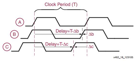
Figure 3. For a periodic signal, an appropriate positive delay can function like a negative delay. Image courtesy of Xilinx.
PLL-Based Clock De-skew
Instead of using a DLL, we can use a PLL to effectively eliminate the delay of the clock distribution network. This is illustrated in Figure 4.
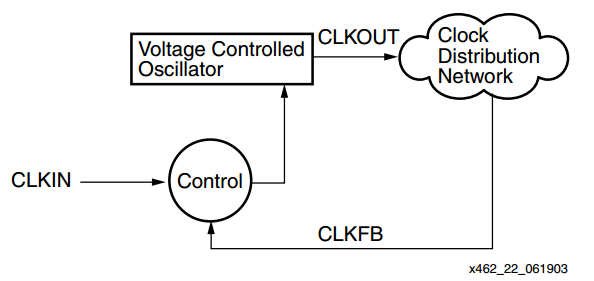
Figure 4. PLL-based clock de-skew. Image courtesy of Xilinx.
In this case, a “Voltage Controlled Oscillator” is used instead of a “Variable Delay Line”. The feedback loop adjusts the frequency of the oscillator such that the two clock signals CLKIN and CLKFB have aligned edges.
We can easily stabilize the feedback loop of a DLL; however, this is not the case with a PLL, because the clock distribution network will be within the PLL's feedback loop. That’s why a DLL-based structure more easily lends itself to clock de-skew applications. On the other hand, a PLL is more flexible when synthesizing new clock signals.
Based on our discussion, we can use the CLBs of FPGAs to de-skew clock distribution of Figure 1 as shown in the simplified block diagram of Figure 5 below. Note that the CMBs can de-skew not only the clock signals distributed within the FPGA but also the clocks going to other devices on the board.
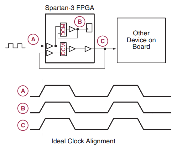
Figure 5. Using CLBs to perform clock de-skew. Image courtesy of Xilinx.
We saw that the CMBs can be used to synthesize new clock signals. Now, let’s look at another group of clock-related FPGA resources: the dedicated buffers and routes that can be used for distributing the clock signals in the FPGA.
Clock-Related Buffers and Routes
These resources are responsible for distributing high-fanout clock signals with a low skew. Going through the details of these buffers and routes can be overwhelming but we’ll have a brief review of some important concepts. To distribute a clock signal to all parts of a chip with equal propagation delays, we can use a special form of routing called an H tree. You can see an example in Figure 6.
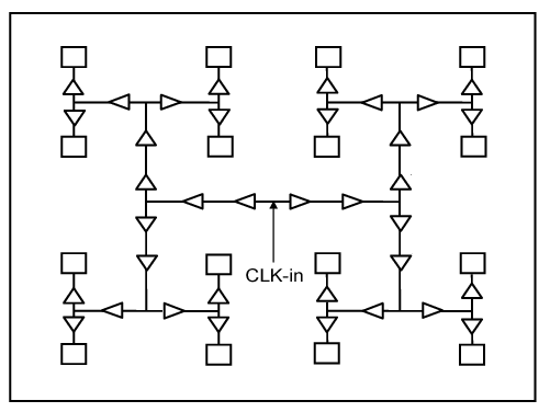
Figure 6. An H tree. Image courtesy of IEEE.
You can easily verify that there’s a similar path from CLK-in to each of the rectangles (which represent a clocked element). Therefore, theoretically, all the clocked elements will see the same clock signal. Figure 7 shows the H tree that some Intel FPGAs use to distribute a global clock signal (GCLK).
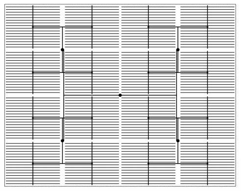
Figure 7. Image courtesy of ACM.
GCLKs are driven throughout the device and serve as low-skew clock sources for functional blocks such as adaptive logic modules (ALMs), digital signal processing (DSP) subcircuits, embedded memory, and PLLs.
In addition to GCLKs, there are regional clock (RCLK) networks in the Intel FPGAs. As shown in Figure 8, these RCLKs are driven into only one quadrant of the chip.
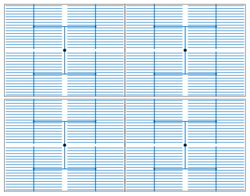
Figure 8. Intel quadrant clock networks. Image courtesy of ACM.
The Intel devices also have periphery clock (PCLK) networks that are distributed in a smaller area of the chip. An example is shown in Figure 9 below.
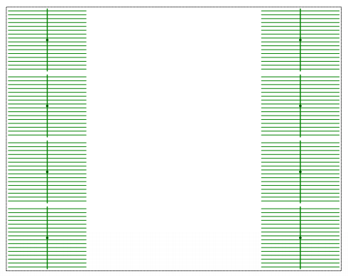
Figure 9. The Intel periphery clocks. Image courtesy of ACM.
Now, overlaying all of these networks, we get the network shown in Figure 10.
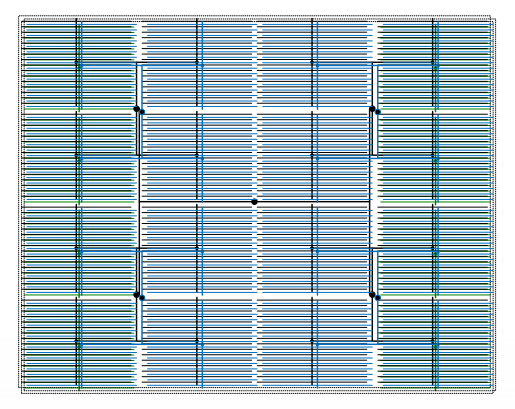
Figure 10. The clock network of an Intel FPGA combines GCLK, RCLK, and PCLK networks. Image courtesy of ACM.
As shown in Figures 8 and 9, FPGAs have dedicated clock routes that are distributed in just one region of the chip. These are called clock regions. Note that different devices have different clock regions. Also note that we need some buffers to efficiently distribute a clock signal along the dedicated routes that we discussed above. You can find the details in your device datasheet, but one example is shown in Figure 11. This figure shows one clock region of a Xilinx 7 series FPGA. BUFG, BUFH, and BUFR are three clock-related buffers that are shown in the figure.
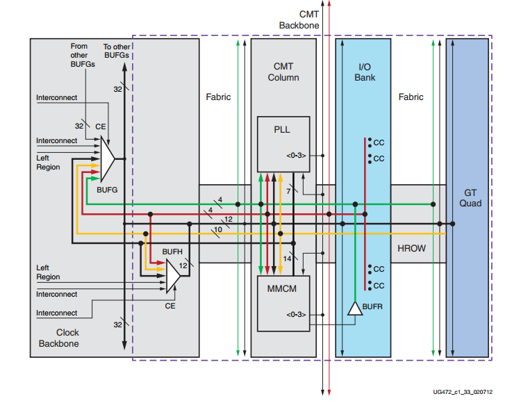
Figure 11. There are several clock-related buffers in each clock region of the Xilinx 7 series FPGAs. Image courtesy of Xilinx.
Here are some concluding notes on FPGA clock resources:
- We can use the clock-related buffers to dynamically enable and disable the clock of a particular region of the chip. This clock enable option can be used as a clock gating technique to reduce the power consumption of a design. For more details refer to the Xilinx 7 series Clocking Resources User Guide or Intel’s Clock Control Block IP Core User Guide.
- The number of high-performance buffers and routing resources are limited, so they should be carefully managed. If there are several clocks in your design, try to assign high-speed and high-fanout clocks to higher-performance global clock routes and resources. For more details, refer to Chapter 9 of Rapid System Prototyping with FPGAs: Accelerating the Design Process.
To see a complete list of my articles, please visit this page.
Related Content


Great post. It should be noted. I would like to add the DFT challenges into it which can be faced by engineers in phase shifted clocks. Learn more: http://bit.ly/2U42qBR