 Facebook
 Google
 GitHub
 Linkedin
What is Clock Skew? Understanding Clock Skew in a Clock Distribution Network
Learn about clock skew, what it is, and its impact on modern systems through understanding synchronous circuitry, clock delivery, and clock distribution networks.
One of the biggest challenges in the design of modern digital electronics is the ability to meet timing constraints. One way to maintain a predictable and well-organized logical flow of operations is to have well-controlled, well-defined timing in a digital circuit.
Clock skew is a design consideration in these circuits that can be a significant source of trouble if not accounted for appropriately. In fact, in many cases, the clock skew of a system can be the limiting factor on overall system speed and clock frequency. To understand clock skew, we must first discuss synchronous circuits.
Synchronous Circuitry and Clocks—Minimum Clock Period Calculation
A fundamental characteristic of most modern digital computers is synchronous circuits.
A synchronous circuit requires a time-keeping mechanism to keep an orderly and periodic sequential logic flow. In digital electronics, this time-keeping mechanism is known as a clock, which, at its simplest, is a square wave with a constant frequency.
As shown in Figure 1, these circuits work by having data at rest stored in data registers designed to latch the data until the register encounters the rising (or falling) edge of the clock. When the clock edge occurs, data is released from the register, sent through combinatorial logic blocks, and then stored at the next register.
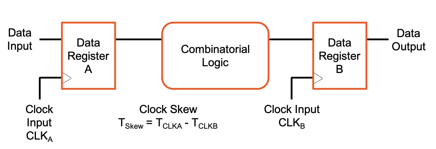
Figure 1. Data path synchronous circuit with two sequential registers.
The frequency with which these operations occur is set by the clock frequency, which is set by several other parameters. The general equation for the minimum clock period is defined as:
$$T_c = t_{pcq} + t_{pd} + t_{setup} + t_{skew}$$
Where:
- Tc is the clock period
- tpcq is the data register clock-to-Q time
- tpd is the combinatorial logic propagation delay
- tsetup is the setup time of the downstream register
- tskew is the clock skew between the two registers
- The maximum clock frequency is defined a $$\frac{1}{T_c}$$
Clock Delivery and Clock Skew
Since digital logic tends to be synchronous circuitry, the precise timing of all logic blocks is crucial to proper system behavior. When you consider scaling the setup in Figure 1 from one data path to millions of data paths (as it exists in real chip design), it quickly becomes obvious that keeping everything synchronized is a non-trivial challenge.
In practice, clock signals are often generated by a crystal oscillator, fed into a phase-locked loop (PLL), and distributed throughout the IC to each logic block and transistor within the system. One of the biggest challenges in this pursuit is known as clock skew, which can be defined as the difference between the clock signal arrival time of sequentially adjacent registers.
This situation can be defined mathematically as:
$$Clock \hspace{.15cm} Skew \hspace{.15cm} = \hspace{.15cm} Receiving \hspace{.15cm} Register \hspace{.15cm} Clock \hspace{.15cm} Delay \hspace{.15cm} – \hspace{.15cm} Transmitting \hspace{.15cm} Register \hspace{.15cm} Clock \hspace{.15cm} Delay$$
The traditional setup in which clock skew occurs is shown in Figure 2, where a delay in the clock distribution network causes data register B to receive its clock signal later than register A.
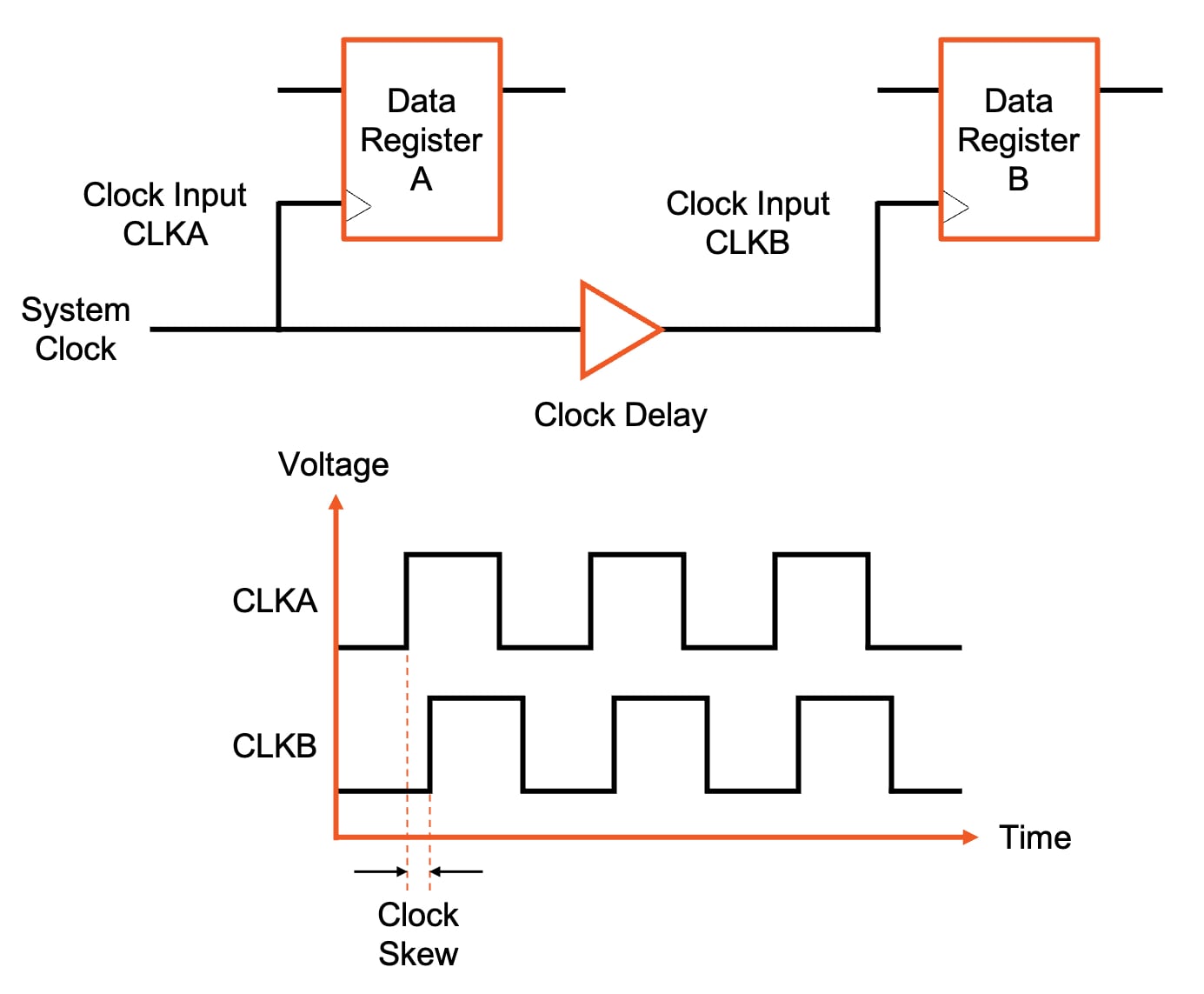
Figure 2. Clock skew is demonstrated by the insertion of a delay in the clock’s delivery network.
Skew can be defined as positive if the receiving register receives the clock later than the transmitting register or negative in the opposite case. Clock skew becomes a serious problem in digital design as it can violate the timing constraints that the synchronous circuits rely on.
For example, given a constant clock frequency and negative skew, as shown in Figure 3, the clock arrives at the receiving register B much earlier than the transmitting register A. In this case, the data sent out from the transmitting register will arrive at the receiving register after the clock arrives. Here, the data does not meet the setup and hold requirements of the receiving register (i.e., the data was not readily available at the receiving register at the time of clock arrival). Due to this, data will be lost since the receiving register cannot latch the data securely. This concept would then have a compounding effect, as future logical operations that rely on the lost data would also fail.
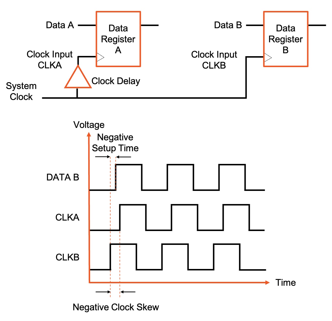
Figure 3. Negative clock skew causes the data to arrive at the receiving register B after its clock.
As we saw in the equation for maximum clock frequency, an increase in clock skew will increase the minimum clock period and reduce the maximum clock frequency of the system. This is because clock skew effectively adds to the sequencing overhead, reducing the time available for useful work in the combinational logic. It is also worth noting that clocks don’t need to be delivered simultaneously, but there is often an acceptable margin of error for clock skew.
Causes of Clock Skew
While there are many causes of clock skew, they all ultimately boil down to differences in delay in the clock distribution network.
One cause of clock skew is differing lengths between interconnects in a clock distribution network. Clock skew can occur if the length of the interconnects in the clock delivery paths to two sequential registers varies significantly. The clock traveling along the shorter interconnect will arrive at its register sooner than it traveling along the longer interconnect.
Another cause of clock skew can be differences in the interconnect delays along the clock distribution network. Even if two clock delivery paths are identical in length, they can experience different delays due to parasitics such as resistance, capacitance, or inductive coupling. In the example of Figure 4, any differences in RC parasitics will result in different delays in the clock arrival times are registers A and B. The clock signal on the line with greater delay will naturally arrive at its destination later than the signal with less delay. Designing interconnects to have equal delay can be an extremely difficult task.
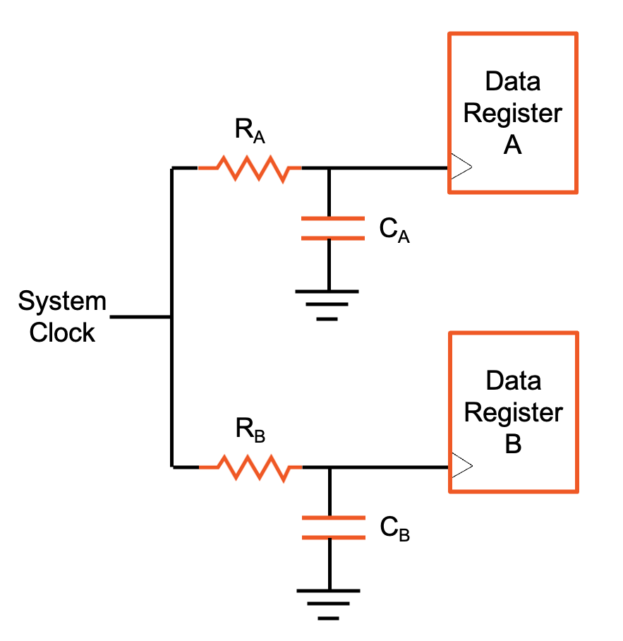
Figure 4. Variations in RC parasitics can cause clock skew.
Clock skew can also be caused by differences in the delay of logical paths for the clock signals. For example, in designs that include clock gating, extra gates may exist in the delivery path of the clock, each featuring its own load capacitance and propagation delay. If not balanced, the differences in logical paths can lead to unequal clock delivery times.
Other causes can include temperature variations, manufacturing variations, and material imperfections.
Minimizing Clock Skew With Clock Distribution Networks
Clock skew can become a more challenging problem as clock frequency increases, as the margin for error significantly decreases with a higher clock frequency. To minimize clock skew, complex synchronous circuits employ clock distribution networks similar to the one shown in Figure 5. These are often also referred to as clock trees. Each inverter in the clock tree amplifies the clock signal to drive the next level of the clock tree. The goal is to have the clock signal simultaneously arrive at all register inputs.
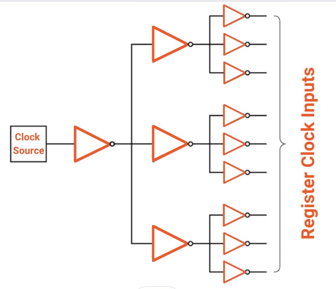
Figure 5. Example of a clock distribution network with parallel clock drivers.
For very large ICs with millions and even billions of transistors, the clock distribution networks can become much more complex than the simple example of Figure 4. The creation of these networks is typically handled automatically by electronic design automation (EDA) software. The engineers enter key parameters like target frequency, register setup and hold time limits, and maximum clock skew. The software then generates a clock distribution network to meet the target timing constraints.
Conclusions
Clock skew is an important topic to consider in digital integrated circuit design. When not properly accounted for, clock skew can wreak havoc on system performance, causing the improper operation of a system, the loss of data, or serving as the limiting factor on system clock frequency.


Even with a pure resistive network, we can get some “skewing”.
Take a mental picture of the ascending front of the signal which is almost vertical for a scope set in the micro-second scale, but becomes almost horizontal in the nano-second scale.
If that slope of the clock front signal is different between two paths due to a resistor, the exact timing when the signal reaches 0.3 volt could be dramatically different on the low resistance and on the high resistance, a little bit as when we switched from the micro to the nano scale. The perception of “when” the signal reaches a logical high can thus be with a delay of few nano-seconds, simply because the rising slope is different, which could be enough to be almost a period later on the higher resistive path. And that, even before considering any capacitance.
Anyhow, that is impressive to see that we have software which can handle these subtilities, considering manufacturing tolerances and a multi-stages multi-components network.