Facebook
 Google
 GitHub
 Linkedin
Designing for Manufacturability
A guideline for proper considerations when making electrical platforms that can be easily, cheaply, and quickly manufactured. The purpose and methods of proper board design, validation, testing, and technical support is discussed, from small to large scale production.
How to make electrical platforms that can be easily, cheaply, and quickly manufactured.
Let's say you have a great idea. It involves electronics, it works, and it will sell. You have it and people want to buy it. You created a schematic, a few prototypes, and an estimate of your return on investment. Let's make some money and get this thing into people's hands!
In terms of manufacturing, however, you've got nothing.
There is a huge gap between a great idea coming from a great engineer--even if you have a fleshed-out concept--and being able to make one thousand or one million of the product. With software, it's easy, but with hardware? It's a long road fraught with peril, paperwork, and painful design revisions unless you do it right the first time. Properly planning your electronic designs is critical. Proper consideration of large-scale production for the design is even more critical.
Your first two decisions are between basing your design around a prototype board or a printed circuit board, and between using through-hole components, surface mount devices (SMDs), or a mix of both.

Typical PCBs.
Prototype boards are generally cheaper for small-scale production because they don't require expensive specialized equipment, while PCBs require investments in either a solder mask machine, a pick-and-place machine, and a reflow soldering oven, or a third party to do it all for you. This greatly increases up-front costs, so surface mount boards are usually more expensive unless you will be making tens of thousands of boards. Designs that use prototype boards can be quickly and cheaply made from parts you can get at a local tech store and don't require proficiency with electronic design automation software (i.e. CAD for electrical engineers); however, a robust PCB design is more flexible in cost requirements for large-scale board productions.
The first step is usually determining if one method simply won’t work for your design due to some external constraint, such as your company’s usual methodology. If both methods are available to you, an informed engineering decision should be based off of cost estimations for each method. However, some designs are cheapest when they use both methods: through-hole components for large resistors and capacitors, and surface mount components for integrated circuits and low power consumption parts.

Through-hole components.
Much of the miniaturization of modern electronics comes from well-designed and extremely specialized printed boards that are “custom-made” instead of prototype boards that use exclusively through-hole parts. PCBs can be made to be very compact using surface mount devices that come in a variety of sizes, including resistors as small as a fifth of a millimeter wide and integrated circuits that have more than 100 pins in a square inch. Integrated circuits for prototype boards are typically limited to dual-inline packages (DIP-xx, for the number of pins they have) whose pins are much larger than the pins available for ICs on PCBs. These IC packages can have a much higher concentration of pins for a given surface area by putting huge arrays of pins *under* the package itself, which are then secured during the specialized reflow soldering process that PCBs undergo. Except when the large size of through-hole parts comes in handy for heat dissipation purposes, it is typically better to use PCB and SMD boards for massive automated production.

Typical SMD board.
There are several aspects of PCB-based design that require special attention during the design phase. While prototype board dimensions are predetermined by the vendor, a designer is free to choose any size trace (a PCB wire) and any distance between traces or components on PCBs. With complete flexibility in the range of possible layouts, the properties of your circuit's signals and the physical board structure make it necessary to design and arrange your board with caution. For example, signals that are very sensitive to noise should not run closely to any power supplies, high current, or magnetic components, and there is a limit to how close two traces can be. Component pads should be properly sized so that the correct part can fit on them without overhanging onto another pad. Holes that are to be drilled in your board and plated vias that carry signals from one plane to another need to be properly measured and have a maximum tolerance associated with them before being finalized. A via that is too small might not receive the correct amount of copper plating to conduct its signal, while a hole that ends up being too large might clip or destroy a nearby pad. Considering possible manufacturing errors in the creation of the printed board is also a critical step in making sure that your layout will meet specifications. There is a huge number of factors, both electrical and mechanical, that constrain the physical layout of your board and require a thorough understanding of what restrictions apply to your design. Ultimately, it is impossible to replace experience with the board layout process with anything but taking the time to layout a board.
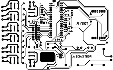
Typical board layout.
After creation of the printed boards themselves, the next step is to apply the silk screen and add components. In support of this manufacturing step, your boards should be clearly labeled to assist with assembly, revision and part numbers, and part outlines. While someone with technical knowledge of the board should be available to the manufacturers, incorporating that information into the board itself easily prevents many common issues. Make sure that the technicians, assemblers, and anyone else who might see or handle the PCBs can easily find out what the product is, what stage it is in, how it should be oriented for assembly, and whether or not the parts have been correctly placed onto the board. Remember that your board text for the manufacturers is sometimes your only form of communication with them, and even a slight error can make an entire board or panel of boards worthless.

Making sure the PCB's text is correct is vital to the success of your project.
However, if the error is not discovered until the board has been shipped to its application the consequences are far more dire. Oftentimes the best case scenario is that your company disappoints a customer and has to pay for potentially thousands of dollars in shipping and part costs, while the worst is loss of life. Efficiently yet reliably testing your board and making a plan, whether cursory or extensive, to validate that your boards are ready for their application is a key step in the overall engineering design process.
One of the more straightforward methods of testing involves simply placing your product into its application before it leaves the manufacturing center. This will work for simple electronics like lights, power supplies, and analog devices, but it is not sufficient to prove that your design can withstand repeated use, “the test of time”, or complex user interface. This method may also not be efficient for large quantities of product, or when the product is time-consuming or difficult to place into its application. Common industrial practice is to build test fixtures, which might be a design project of their own, that can easily provide a range of inputs and clearly indicate success or failure to the tester. Consider the advantages of creating a specialized bed-of-nails device which can easily and simultaneously test all boards from a PCB batch.
The bed of nails test.
For products that must be durable to human interaction or withstand many hours in the field, it is often best to take a small sample of each batch and stress test them in a shortened time frame or begin conducting tests before the product will be available for sale. Many advanced systems like computers, avionics, and mobile devices are too flexible to possibly test all possible conditions and inputs at a hardware level and require more thorough validation. These products must be designed to withstand varying inputs and have built in safety factors to misuse and still must be tested thoroughly in their applications.
Once the design has been set and the time comes to start making trial runs of your product, the role of the designer backs off, and the role of the manufacturer takes over. The engineer, while continuing onto the next project, must still support the project as it transitions from design to product. Ask yourself, or others, how you can help. There will be issues at every stage of the process. Maybe the company who makes the boards doesn't have the capability to drill holes of the size you want for a set of pins. The component supplier ran out of your power supply device right before getting to your order. The company who places components onto your board can't seem to get R1, R3, and D2 to solder well to the pads. Unforeseeable circumstances are hard to avoid but proper oversight eases this process.

Testing with a multimeter helps problems down the road.
Remember to always validate your testing periodically; simple checks from a human being can go a long way. Hiring a person with a multimeter to check continuity between two points in a circuit, even if he only touches 1% of your product is a simple way to make sure you don't get an angry call from a customer. Visiting the manufacturing center and testing that your test fixtures themselves still work after a few months can prevent thousands of dollars of loss. Manufacturing groups may or may not have the capability to discover or solve these problems before they become a massive pain for you, and it is up to you to be a pair of watchful eyes as work on the product is taken from your hands and given to the manufacturer.
Related Content