Facebook
 Google
 GitHub
 Linkedin
How Does Xilinx Use Its Logic Fabric to Implement Efficient Multipliers?
This article will review the structure of the binary multipliers that use the look-up tables (LUTs) in the Xilinx logic fabric.
This article will review the structure of the binary multipliers that use the look-up tables (LUTs) in the Xilinx logic fabric.
Nowadays, FPGAs are widely used for digital signal processing applications. Such applications commonly require multiplication operations. That’s why today’s FPGAs have several embedded hard multipliers distributed throughout the chip.
Sometimes, though, we need to have a more flexible multiplier. To this end, we can use soft multipliers that allow us to choose factors such as the size of the operands and the location of the multiplier on the chip.
It should be noted that researchers are still working on the design of LUT-based soft multipliers. For a review of recent work, you can refer to this open access paper: "Array Multipliers for High Throughput in Xilinx FPGAs with 6-Input LUTs" by E. George Walter, published in the journal, Computers. The paper also presents an advanced LUT-based multiplier. Such designs are beyond the scope of this article, but we will review a basic LUT-based multiplier structure that can be automatically inferred from a multiplication operator (*) by the synthesis tool [1].
An Efficient Design Must Consider the FPGA’s Logic Fabric
There are numerous structures, with different complexities and delays, that can be used to implement a binary multiplier. For example, when multiplying the two four-bit numbers shown in Figure 1, we can use logic gates to generate the partial products and then add them together to find the product.
Such implementations are possible, but they are not necessarily efficient because they don’t make use of the special logic fabric available in the FPGA. The Xilinx configurable logic block (CLB) incorporates a fast carry chain that allows for the implementation of efficient multipliers. In the rest of this article, we’ll first review the basic CLB structure and then we’ll see how this structure can lead to an efficient multiplier.
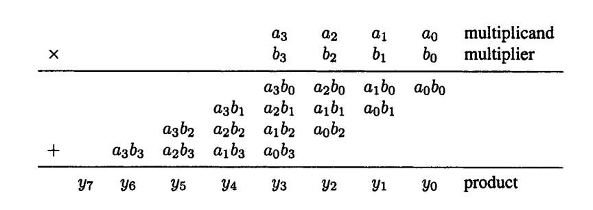
Figure 1. Multiplication of two four-bit numbers. Image courtesy of RTL Hardware Design.
The CLB Structure of Early Virtex Devices
Each CLB consists of slices, and a slice is composed of smaller units. For example, in older Xilinx technology, a slice consists of two of the circuits shown in Figure 2. Note that this circuit is a simplified version of the real implementation. The circuit is designed to achieve fast implementations of certain arithmetic functions such as addition and multiplication.
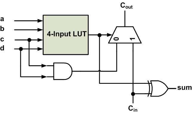
Figure 2. The simplified structure of half a slice.
Let’s see how the circuit of Figure 2 can be used to implement arithmetic functions efficiently.
Implementing Addition
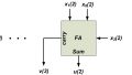
In a previous article, I explained how to use VHDL components to create a neat hierarchical design. In that article, we saw that to add two n-bit numbers, we can use a cascade of n full adders (FAs).
The truth table for generating the sum and carry outputs of an FA is given in Table 1. The table also shows the values for another signal, $$P_i = A_i \oplus B_i$$, which we'll discuss in a minute.
Table 1
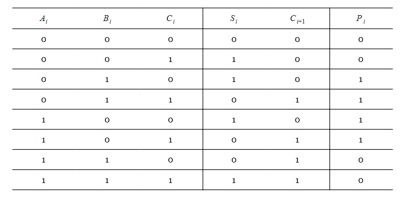
Here, $$A_i$$ and $$B_i$$ are the digits of the ith column of addition and $$C_i$$ is the carry produced by the previous column. Adding these three bits gives a sum, $$S_i$$, and a carry $$C_{i+1}$$. $$C_{i+1}$$ will be added to the digits of the next bit position. Based on the truth table, we obtain the following expressions:
$$S_i = A_i \oplus B_i \oplus C_i$$
$$C_{i+1} = ( A_i \oplus B_i ) C_i + A_i B_i$$
To implement these two expressions using the circuit of Figure 2, we first realize the expression $$P_i = A_i \oplus B_i$$ using the look-up table of Figure 2. The LUT has four inputs and can implement any four-input logic function. Now, we have
$$S_i = P_i \oplus C_i$$
$$C_{i+1} =P_i C_i+A_i B_i$$
As you can see, the XOR gate of Figure 2 implements the sum equation (one of its inputs comes from the LUT ( $$P_i$$ ) and the other input comes from the carry produced by the previous bit position).
To implement the carry equation, note that when $$P_i = 1$$, we have $$C_{i+1}=C_i$$. You can verify this from the above truth table. Also, when $$P_i = 0$$, $$C_{i+1} = A_i = B_i$$. In Figure 2, when the output of the LUT is high ( $$P_i = 1$$ ), the multiplexer will pass the input carry, $$C_{in}$$, to $$C_{out}$$. When $$P_i = 0$$, the output of the AND gate must be equal to either $$A_i$$ or $$B_i$$.
It should be noted that we could actually implement addition without even using the AND gate in the circuit of Figure 2. The AND gate is mainly used to facilitate implementing multiplication, which will be discussed in the next section.
With the explained configuration, the circuit of Figure 2 can implement an FA. This one-bit addition can be extended to n-bit addition by cascading FAs. Note that the carry logic uses dedicated circuitry to speed up carry propagation.
Implementing Multiplication
Interestingly, the carry logic incorporated in a slice can be used to efficiently implement multiplication too. Consider the 4-bit by 2-bit multiplication below:
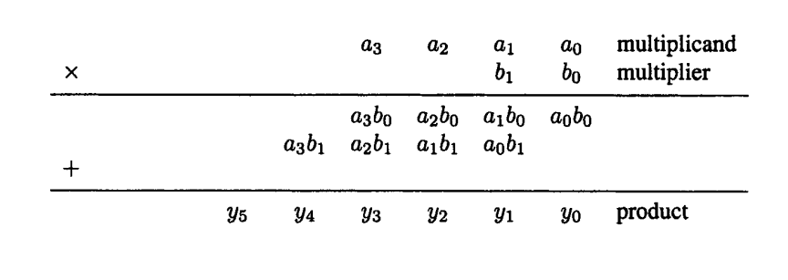
The least significant bit of the product can be obtained simply by ANDing $$a_0$$ and $$b_0$$. Let’s consider the third bit of the product, i.e., $$y_2$$. To obtain this bit, we should add $$a_2 b_0$$, $$a_1 b_1$$, and the carry from the previous column. It seems that the Xilinx carry logic can be used to implement this FA. We’ll see that the Xilinx logic fabric has more than this to offer. And a more efficient implementation can be achieved by means of the four-input LUT and the AND gate (see Figure 2).
Let’s assume that we want to use the circuit of Figure 2 to add the values $$a_2 b_0$$, $$a_1 b_1$$, and the carry from the previous column, $$C_{in}$$. Based on our discussion about addition, we can define a $$P_2$$ signal equal to $$a_2 b_0 \oplus a_1 b_1$$. Since the LUTs have four inputs, we can use them to generate any four-input function. Hence, the $$P_2$$ signal can be produced using a LUT.
We know that when $$P_2 = 1$$, the output carry must be equal to the input carry $$C_{in}$$. The circuit of Figure 2 already takes this into account. When $$P_2 = 0$$, $$C_{out}$$ must be equal to either $$a_2 b_0$$ or $$a_1 b_1$$ (it doesn’t matter which one—if $$P_2 = 0$$, $$a_2 b_0 = a_1 b_1$$) . As shown in Figure 2, for $$P_2 = 0$$, the multiplexer will pass the output value of the AND gate to $$C_{out}$$. Hence, the AND gate must be connected to either ( $$a_2$$ and $$b_0$$) or ( $$a_1$$ and $$b_1$$).
This example shows that we can achieve an n-bit by 2-bit multiplication using almost the same logic resources as required by a simple n-bit adder. When dealing with an n-bit by m-bit multiplication, we can express the multiplication in terms of several n-bit by 2-bit multiplications. Then, we can use a multi-operand adder to add the products obtained from these multiplications. For a block diagram of a four-bit by six-bit multiplier, see Section 12.1.7 of the book Synthesis of Arithmetic Circuits: FPGA, ASIC and Embedded Systems by Jean-Pierre Deschamps, Gery J.A. Bioul, and Gustavo D. Sutter.
The LUT-based multiplier discussed in this article can be automatically inferred from a multiplication operator (*) by the synthesis tool [1]. However, we can also use a custom design such as the one discussed in the paper I mentioned earlier ("Array Multipliers for High Throughput in Xilinx FPGAs with 6-Input LUTs").
Summary
- Sometimes, we need soft multipliers that allow us to choose factors such as the size of the operands and the location of the multiplier on the chip.
- An efficient implementation must consider the logic fabric available in the FPGA.
- The carry logic uses dedicated circuitry to speed up carry propagation and, consequently, the addition operation.
- The carry logic incorporated into a slice can be used to efficiently implement multiplication.
Reference
1- “Guide to FPGA Implementation of Arithmetic Functions” by Deschamps, Jean-Pierre, Sutter, Gustavo D., Cantó, Enrique, 2012.
2- “Synthesis Of Arithmetic Circuits FPGA, ASIC and Embedded Systems” by Jean-Pierre Deschamps, Gery J.A. Bioul, Gustavo D. Sutter, 2006.
3- "Design Tips for HDL Implementation of Arithmetic Functions", by Steven Elzinga, Jeffrey Lin, and Vinita Singhal, 2000.
4- “Array Multipliers for High Throughput in Xilinx FPGAs with 6-Input LUTs” by E. George Walters, 2016.
To see a complete list of my articles, please visit this page.
Related Content