 Facebook
 Google
 GitHub
 Linkedin
How to Design Schmitt Trigger Oscillators
This article discusses the good and the bad regarding Schmitt Trigger RC oscillators. These oscillators are especially important because they are present in the internal oscillator in many popular MCUs.
This article discusses the good and the bad regarding Schmitt Trigger RC oscillators. These oscillators are especially important because they are present in the internal oscillator in many popular MCUs.
In the previous article, Exactly How Schmitt Trigger Oscillators Work, we went over the schematic of a basic RC Schmitt trigger oscillator and derived a general equation for the period and frequency.
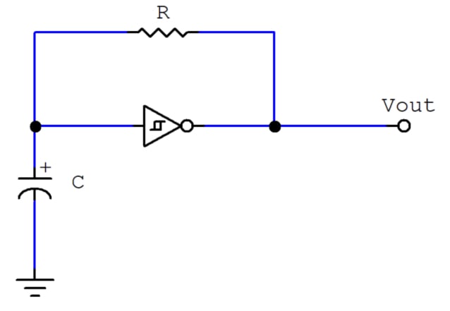
Figure 1. RC Schmitt trigger oscillator
$$T=RC \; ln \left ( {V_{High}-V_{T-} \over V_{High}-V_{T+}} \times {V_{T+} \over V_{T-}} \right ) \\\\$$
Equation 1. The period of the output signal.
$$f={1 \over RC \; ln \left ( {V_{High}-V_{T-} \over V_{High}-V_{T+}} \times {V_{T+} \over V_{T-}} \right ) } \\\\$$
Equation 2. The general equation for frequency.
These equations assume a lot of convenient parameter values, and they’re not completely accurate. For example, the high output voltage is not necessarily the supply voltage. The Schmitt Trigger threshold voltage values may vary from manufacturer to manufacturer. So, there are always extra considerations involved with designing an RC Oscillator.
Not Just Any Schmitt Trigger Gate Will Do
The ln portion of the period and frequency equations is a constant that depends on the threshold voltages. Threshold voltages are specific to the particular integrated circuit used. So, whatever constant that appears in the period and frequency equations varies from chip to chip.
Moreover, the datasheet of either the Schmitt Trigger inverter or gate will establish a range of possible values for $$V_{T+}$$ and $$V_{T-}$$, normally contained within a minimum and maximum specified values. A typical value may also be specified, but there are no guarantees on the actual thresholds your chip will have, other than being within the minimum and maximum. Unfortunately, this part is out of your control.
The 74LS14 Schmitt Trigger Gate IC
A very popular Schmitt Trigger gate IC in the TTL LS family is the 74LS14, which is a set of six inverters, with threshold voltages below 2.5V (which is half the supply voltage). The problem lies in the discharge phase (low pulse width), which takes much longer than the charging phase (high pulse width). This happens because the charge phase is configured to reach from $$V_{T-}$$ to $$V_{DD}$$. This is a much greater initial voltage difference than that of the discharge phase, which is $$V_{T+}$$. Figure 2 shows the situation graphically:
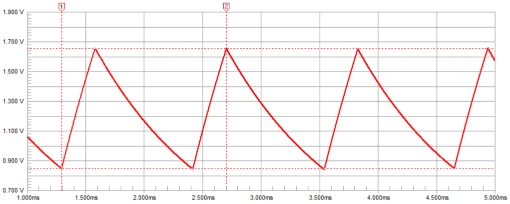
Figure 2. Capacitor voltage of a 74LS14-based RC oscillator. For this gate, $$V_{T+}$$ is 1.66V, and $$V_{T-}$$ is 0.84V.
4093B CMOS Integrated Circuit
Another popular option is the 4093B CMOS integrated circuit, which has threshold voltages much closer to the desired symmetrical thresholds configuration. Figure 3 shows the same graphical situation for the 4093B:
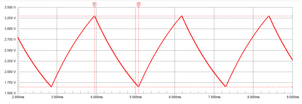
Figure 3. Capacitor voltage of a 4093B-based RC oscillator. For this gate, $$V_{T+}$$ is 3.3V, and $$V_{T-}$$ is 1.65V.
Because the 4093B is a two-input NAND, it can act as the original inverter when the other input is high. This gives the circuit the feature of an enable input line. Whenever this enable line is high, the circuit will output the clock signal, and when it is not, a fixed high value.
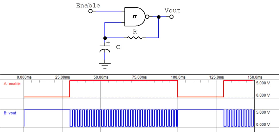
Figure 4. RC oscillator with the 4093B CMOS quad NAND integrated circuit.
In Figure 4, the extra input is used as an enable line. Note that the idle state in the output is high.
TTL vs CMOS
Another reason for using the 4093B IC instead of the 74LS14 is their implementation technology. TTL gates are made with BJTs, and despite the variant used in the LS family is aimed for low power, their input impedance is not very good. These gates can have an input current as high as 1mA and as low as 0.1mA.
CMOS gates, on the other hand, are made with MOSFETs, which have an extremely high input impedance—always higher than $$10M\Omega$$. This results in input currents always lower than 100nA.
The problem with this parameter (input impedance) is that it has an impact on how accurate the series model is for the RC charge/discharge circuit. Having lower input impedances creates a more noticeable load effect on the RC circuit, and a more appropriate model for it would have to account for that lower input impedance.
An implication of using TTL ICs for an RC oscillator is that the value of R is limited to smaller values, typically under $$2k\Omega$$. This forces designers to use bigger capacitors to achieve lower frequencies.
In any case, a CMOS gate does not have this problem.
The Output Will Hardly Be Rectangular
The output voltage produced by the original oscillator is not exactly a rectangular wave. The slope visible in the low and high states is an effect of the analog nature of the feedback loop.
Remember that the capacitor is drawing current from the gate’s high-level output, and providing current to the gate’s low-level output. The cause of the slope is the output impedance of the gate.
Logic gates are generally supposed to provide their outputs to digital inputs, not to power-consuming elements, so the output impedance in these devices isn’t all that low. Thus, the voltage measured at the output pin is the intended output minus the voltage drop in the series Thevenin output resistor. This resistor’s voltage is proportional to the current, which is changing. Figure 5 shows this situation.

Figure 5. The effects of a considerable output resistance.
The gate in the figure above is modeled as a square wave generator with a resistor in series, shown inside the shaded area. The ideal output signal (Vout) is measured at the output of the generator, before the voltage drop in the output resistor, and it’s shown as red in the plot. The actual voltage in the output pin (Vpin) is shown as blue in the plot. Notice how the ideally rectangular signal (red) is deformed in both the high and low levels (blue).
The problem caused by the output resistance is twofold: first, it affects the charge and discharge times, and second, the output signal is not rectangular.
Elaborating on the first problem, the output resistance causes the output pin voltage to have a lower high-level voltage and a higher low-level voltage. This means that the charge and discharge equations will not be very accurate after all because the voltage differences will actually be smaller. A simple solution to this inaccuracy is to learn the value of the output resistance from the datasheet and add it to the value of R.
$$RC \rightarrow (Rout+R)\times C$$
As for the second problem, having a non-rectangular signal is not usually bad for a digital input. However, connecting anything else to the output will have an effect on the behavior of the oscillator because the output will be further loaded. A good practice is to leave the oscillating part to itself and regenerate that signal with one of the remaining gates in the integrated circuit. This is done primarily to regenerate the output signal for whatever digital circuit is supposed to use it.
In the case of a NAND oscillator, this second inverter stage will also leave the “idle” state as low instead of high. So, depending on the designer’s preference, another inverter may be required. Figure 6 shows a circuit with all the improvements mentioned.
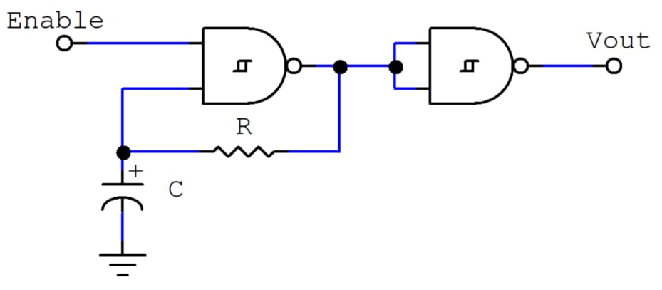
Figure 6. A practical 4093B Schmitt Trigger RC oscillator with an output suitable for feeding into digital inputs, and a low idle state.
The 555 Timer
The 555 timer is by far the most popular analog integrated circuit for generating low-frequency clock signals with modest requirements.
The principle of operation for a 555 timer as an astable multivibrator is, in essence, the same as the Schmitt Trigger RC Oscillator’s because it maintains a capacitor’s voltage between two levels, typically 1/3 and 2/3 of VDD respectively.
The 555 timer’s astable circuit can only generate signals with a duty cycle greater than 50%. However, it is possible to reach any duty cycle with some modifications. Likewise, the Schmitt Trigger RC oscillator generates signals with some fixed duty cycle (50% for symmetrical hysteresis) but can be modified to generate just about any duty cycle. Rectifiers usually do the trick for both circuits.
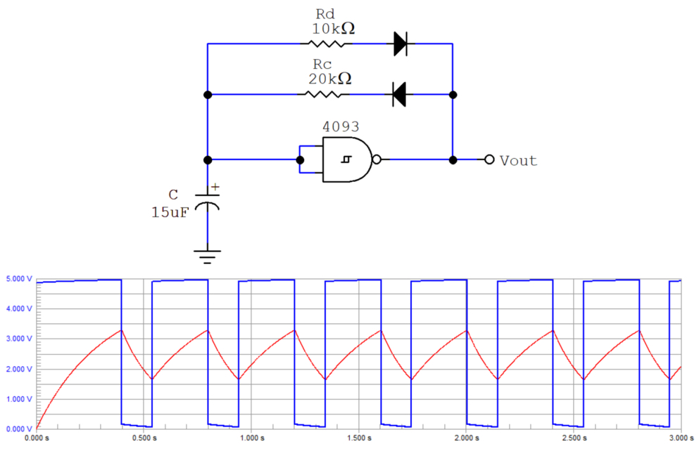
Figure 7. RC oscillator with separate charging and discharging resistors.
Notice how Figure 7 shows the capacitor charges through Rc and discharges through Rd. This separates the control of th and tl for generating any duty cycle. In this circuit, the NAND gate implements a single-input inverter.
Also, modifying the pulse width while keeping the period constant is required for pulse width modulation. This can be achieved by both circuits using a potentiometer where the resistors are.
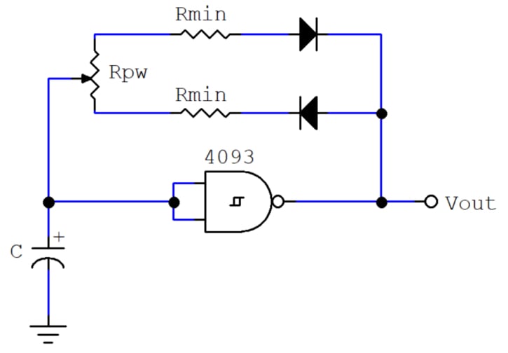
Figure 8. A PWM generator implemented with an RC oscillator.
Notice that in Figure 8, the potentiometer acts as both the charge and the discharge resistors in the previous circuit. The two fixed resistors must have a resistance that yields the minimum desired value of th and tl respectively. These resistors are mandatory because setting the potentiometer at either end would make the RC circuit’s effective resistance too low (just the output resistance of the gate plus the diode’s forward resistance), which may make the gate’s output current approach it's maximum rating.
Conclusion
The accurate design of an RC oscillator depends on a series of parameters specific to the components present in the implementation. However, the circuitry is so simple that the inaccuracies in their design can be overcome by trial and error. For example, if the values of R and C may be set by the simplified equations, then the resulting frequency can be trimmed by varying the resistance or capacitance. Actually, a trimming potentiometer is often used to fine-tune the generated frequency.
When it comes to an astable multivibrator (generating a clock signal with modest frequency accuracy), the 555 timer doesn’t offer a dramatic advantage over the very simple Schmitt Trigger oscillator.
Related Content


Nice content!
RE; Figure 7. RC oscillator:
Looks to me like the circuit is designed to work with the 4093 with a +/- supply.
With a +/gnd supply the amount of feedback will be different in the two halves of the cycle. Which might be ok since one can set the FB resistors accordingly.
Eduardo,
Brilliant article. I will site this in an upcoming post on a capacitor ESR meter that this was an integral part of. Thanks for the detail!
Thank you,
glydeck