 Facebook
 Google
 GitHub
 Linkedin
Integrator Limitations: The Op-Amp’s Gain Bandwidth Product
In this first part of a series of articles, we investigate the role of the op-amp’s gain-bandwidth product (GBP).
In this first part of a series of articles, we investigate the role of the op-amp’s gain-bandwidth product (GBP).
The op-amp integrator lends itself to a variety of applications, ranging from integrating-type digital-to-analog converters, to voltage-to-frequency converters, to dual-integrator-loop filters, such as the biquad and state-variable types. These systems are usually analyzed by assuming ideal integrator behavior, when in fact there are limitations stemming primarily from op-amp nonidealities, that the user needs to be aware of for an effective application of the integrator.
In this first part of a series of articles, we investigate the role of the op-amp’s gain-bandwidth product (GBP).
Integrator Using an Ideal Op-Amp
Let us briefly review the ideal integrator, so we have a standard against which to compare a real-life integrator. For a thorough comparison, it pays to investigate the integrator both in the time domain and in the frequency domain.
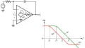
For time-domain analysis, refer to Figure 1(a).
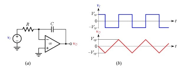
Figure 1. (a) Integrator and (b) example of time-domain integrator behavior.
Exploiting the fact that an ideal op-amp keeps the inverting- input node at virtual ground, or 0 V, we apply KCL to write
\[\frac {v_I - 0}{R} = C \frac {d(0- v_O)}{dt}\]
or
\[dv_O = \frac {-1}{RC} v_I dt\]
Integrating both sides from 0 to t,
\[\int_{0}^{t}dv_O = \frac {-1}{RC} \int_{0}^{t} v_I dt\]
and considering that the left-hand term reduces to \(v_O (t) – v_O (0)\), we finally get
\[v_O(t) = \frac {-1}{RC} \int_{0}^{t} v_I (t)dt + v_O(0)\]
Equation 1
In words, \(v_O (t)\) is proportional to the integral of \(v_I(t)\), with the constant of proportionality being –1/RC. Moreover, \(v_O(0)\) is the initial value, which depends on the charge Q(0) initially stored in the capacitor as \(v_O(0) = Q(0)/C \). A good way to evaluate an integrator in the time domain is via the quality of the ramps it generates in response to constant input voltages, such as those exemplified in Figure 1(b).
For frequency-domain analysis, refer to the circuit of Figure 2(a).
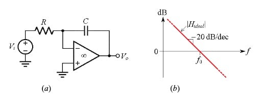
Figure 2. (a) Integrator and (b) its ideal gain, or transfer function \(H_{ideal}(jf)\) in the frequency domain.
Applying the gain formula of the ideal inverting amplifier, we write the ideal transfer function as
\[H_{ideal}(s) = \frac {V_o}{V_i} = - \frac {1/(sC)}{R} = \frac {-1}{sRC}\]
Equation 2
where s is the complex frequency, and \(V_i\) and \(V_o\) are the Laplace’s transforms of the input and output voltages. Plotted in the s-plane, \(H_{ideal}(s)\) looks like a tent with a single pole pitched right at the origin. We are primarily interested in the frequency-domain (or ac) response, so we limit our considerations to the tent’s profile along the imaginary axis, which we obtain by letting \[s\rightarrow j\omega\], where ω is the angular frequency. (Actually, in the lab and in the course of SPICE simulations we work with the frequency \[f = \omega/2\pi\], in Hertz.) So, letting \[s\rightarrow j\omega = j 2\pi f\], we put Equation (2) in the more insightful form
\[H_{ideal}(jf) =\frac {V_o}{V_i}= \frac {-1}{jf/f_0 }\]
Equation 3
where \(V_i\) and \(V_o\) are the phasors associated with the input and output, and
\[f_0 = \frac {1}{2 \pi RC}\]
Equation 4
The magnitude plot of \(H_{ideal}\) vs. f is a hyperbola, but when plotted on logarithmic scales it becomes a straight line with a slope of –20 dB/dec, as shown in Figure 2(b).
For obvious reasons, \(f_0\) is called the integrator’s 0-dB gain frequency, or also the unity-gain frequency.
Integrator Using a Constant GBP Op-Amp
Real-life integrators are usually implemented with constant gain-bandwidth product (constant GBP) op-amps. With reference to the integrator of Figure 3(a), where the op-amp’s gain is denoted as a, we seek a closed-loop transfer function of the type
$$H(jf) = \frac {V_o}{V_i} = H_{ideal}(jf) \frac {1}{1+1/T (jf)}$$
Equation 5
where \(H_{ideal}\) is as in Equation (3) and T = aβ is called the loop gain.
Moreover, β is called the feedback factor. We find it by setting the input to zero, breaking the loop at the op amp’s output, and applying a test voltage \(V_t\) as shown in Figure 3(b).
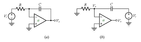
Figure 3. (a) Integrator using an op-amp with open-loop gain a ≠ ∞. (b) Finding the feedback factor β.
Finally, we use the voltage divider formula to get
$$\beta = \frac {V_n}{V_t} = \frac {R}{R+1/(j2\pi fC)} = \frac {j2 \pi fRC}{1+ j2\pi fRC} = \frac {jf/ f_0}{1+jf /f_0}$$
Equation 6
with \(f_0\) as in Equation (4).
To construct the Bode plot of |H(jf)|, it is more convenient to work with the reciprocal of β , also known as the noise gain,
$$\frac {1}{\beta} = \frac {1}{jf/f_0}+1$$
Equation 7
for then we can visualize the decibel plot of |T| = |aβ| = |a|/|1/β| as the difference between the decibel plot of |a| and that of |1/β|,
\[\left |T \right |_{dB} = \left | a \right |_{dB} - \left | 1/\beta \right |_{dB}\]
Equation 8
The plots of |a|, |1/β|, and |H| are shown in Figure 4.
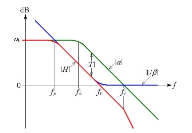
Figure 4. The transfer function |H| of an integrator implemented with a constant GBP op-amp. Here, a is the op-amp’s open-loop gain, \(a_0\) its dc value, \(f_b\) its –3-dB bandwidth, and \(f_t\) its transition frequency. The noise gain 1/β of Equation (7) has a high-frequency asymptote of 1, or 0 dB, and a low-frequency asymptote of 1/(jf/f0), whose magnitude coincides with that of \(H_{ideal}\) of Equation (3).
From this, we make the following considerations:
- T is largest for \(f_b < f < f_0\), so this is the frequency range over which H is closest to \(H_{ideal}\), by Equation (5).
- As we lower f below \(f_b\), |T| gradually decreases until it reaches 0 dB at \(f_p\). Below \(f_p\), C acts as an open circuit, thus letting the op-amp amplify at its full dc gain \(a_0\). To find \(f_p\), we exploit the constancy of the GBP of |H| from \(f_p\) to \(f_0\) and write \(a_0 \times f_p = 1\times f_0 \). This gives \(f_p = f_0/a_0\).
- As we raise f above \(f_0\), |T| gradually decreases until it reaches 0 dB at \(f_t\). For \(f >> f_t\), |T| becomes so small (and 1/|T| so large) that we can approximate Equation (5) as
\[H \cong H_{ideal} \frac {1}{1/T} = H_{ideal}T = H_{ideal}\: a \beta = H_{ideal}\: a \times 1 \cong \frac {-1}{jf/f_0} \times \frac {1}{jf /f_t}\]
indicating that above \(f_t\), |H| rolls off with frequency at the rate of –40 dB/dec.
It is apparent that H has two pole frequencies, so we can also express it in the alternative form
\[H(jf) = \frac {-a_0}{(1+jf /f_p)(1+jf/f_t)}\]
Equation 9
where \(f_p = f_0/a_0\). This is a far cry from $$H_{ideal}$$ of Equation (3). Only in the limits \(f >> f_p\) and \(f << f_t\) will H approach \(H_{ideal}\).
Verification via PSpice
Let us verify our findings via PSpice. The circuit of Figure 6(a) uses a Laplace block to simulate an op-amp with \(a_0 = 10^5\) V/V and \(f_b\) = 10 Hz, so \(f_t\) = GBP = $$a_0 \times f_b$$ = 1 MHz. By Equation (4), the integrator’s unity-gain frequency is \(f_0\) = 10 kHz. Moreover, \(f_p = f_0/a_0\) = 0.1 Hz.
The plots of Figure 5(b) confirm our analysis.
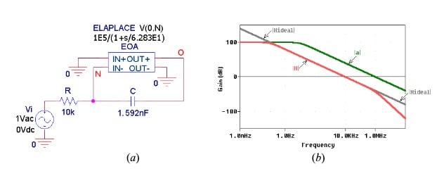
Figure 5. (a) PSpice integrator using a Laplace block to simulate an op-amp with GBP = 1 MHz. (b) Plots of the open-loop gain |a|, the ideal integrator transfer function |\(H_{ideal}\)|, and the actual function |H|.
Next, let us investigate the integrator of Figure 5(a) in a popular real-life application, namely, the actively-compensated biquad filter shown in Figure 6.
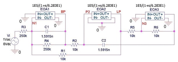
Figure 6. PSpice circuit schematic of an actively compensated biquad filter designed for a band-pass response centered at \(f_0\) = 10 kHz with a quality factor Q = 25.
This filter provides both the band-pass (BP) and the low-pass (LP) responses.
The plots of Figure 7(a) show the two responses for the case of ideal op-amps simulated by changing the dc gains of the Laplace blocks from 1E5 to 1E7, and dropping entirely the denominator polynomial in s. The BP response is symmetric about 10 kHz, with a low-frequency slope of +20 dB/dec and a high-frequency slope of –20 dB/dec. The LP response has a high-frequency slope of –40 dB/dec.
Turning to the real-life plots of Figure 7(b), we observe that the effect of GBP = 1 MHz is to initiate, at about 1 MHz, steeper roll-off rates for both responses, so the ultimate rate for the BP response changes from –20 dB/dec to –40 dB/dec, and that for the LP response from –40 dB/dec to –60 dB/dec.

Figure 7. Band-pass and low-pass responses of the biquad filter of Figure 6 for the case of (a) ideal op-amps, and (b) op-amps with GBP = 1 MHz.
Depending on the application, these steeper roll-off rates may actually be welcome. However, there are also some subtle changes in f0 and Q that will be addressed in a subsequent article.
Stability Considerations
Looking at Figure 4, we note that above f0 we have β → 1. This is so because for \(f >> f_0\), C acts as a short, forcing the op-amp to operate in the unity-gain voltage-follower mode. So, if the op-amp is of the fully compensated type, it will be stable also as an integrator.
Now, considering that for a given \(f_0\), a well-designed integrator should use an op-amp with \(f_t >> f_0\), we wonder whether an integrator can be implemented with a decompensated op-amp, which enjoys a higher ft than its fully compensated version. The integrator of Figure 8(a) uses a decompensated op-amp with a dc gain of 100 dB and a dominant pole of 100 Hz (for a GBP of 10 MHz), plus a second pole at 1 MHz. Its transition frequency is now \(f_t\) = 3.08 MHz, where its phase angle is –162°. The |1/β| curve will still intercept the |a| curve at \(f_t\), so this integrator’s phase margin is \(\phi_m\) = 180 – 162 = 18°, not much of a margin. In fact, if this op-amp were used as a plain unity-gain voltage follower, its ac gain would exhibit peaking of over 10 dB, and its transient response an overshoot of over 60%.
However, the ac response of Figure 8(b) shows a much reduced amount of peaking (about 2 dB), indicating that the integrator, being a low-pass filter, attempts to reduce its own peaking. Just like the integrator reduces peaking in the frequency domain, it reduces also the amount of ringing in the time domain.
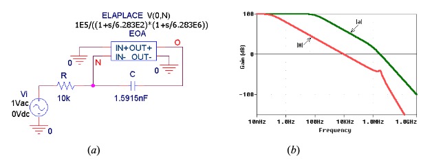
Figure 8. (a) Integrator using a decompensated op-amp having the phase margin \(\phi_m\) = 18°. (b) The low-pass filtering action by the integrator reduces the amount of peaking appreciably.
This is depicted in Figure 9, whose plots are generated by changing the input ac source of Figure 8(a) to a 10-kHz pulse source.
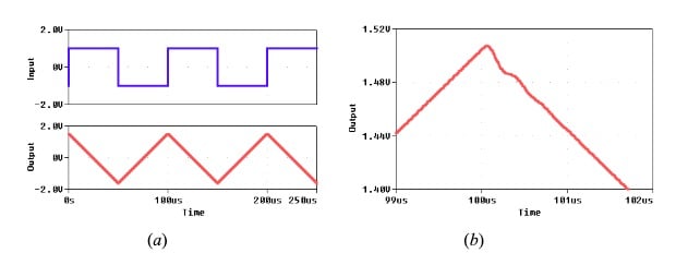
Figure 9. (a) Response of the integrator of Figure 8(a) to a 10-kHz square wave. (b) Expanded view showing a small amount of ringing following an input step change.
In conclusion, the use of decompensated op-amps is generally discouraged, even though in integrator operation both peaking and ringing are reduced considerably.


Excellent article. I wanted to add one thing to the assertion “A good way to evaluate an integrator in the time domain is via the quality of the ramps it generates in response to constant input voltages”. An overlooked error in an op amp integrator is the “voltage coefficient of capacitance” of the feedback capacitor. As the output voltage changes, the capacitance can change, sometimes quite dramatically. The ramp “wanders” from the ideal straight line as the output voltage increases and decreases. Different types of capacitors have different voltage coefficients.