Facebook
 Google
 GitHub
 Linkedin
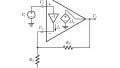
Decompensated Operational Amplifiers
Learn more about decompensated vs. fully-compensated op-amps and external methods of achieving compensation.
Learn more about decompensated vs. fully-compensated op-amps and external methods of achieving compensation.
As discussed in a previous article, Miller frequency compensation makes it possible to use rather small values of the compensation capacitance Cƒ. This is highly desirable not only because Cƒ can be fabricated on-chip, but also because it results in faster dynamics than, say, shunt-capacitance compensation. This is so because the slew rate, the open-loop bandwidth, and the full-power bandwidth are approximately inversely proportional to Cƒ.
Now, compensation for closed-loop gains all the way down to unity gain is the most conservative in terms of the size of Cƒ. There are many applications involving closed-loop gains greater than a minimum, such as greater than Amin = 10 V/V, which would work with an even smaller Cƒ and thus enjoy even faster dynamics.
Let us use our running PSpice circuit example, first introduced in my article on op-amp frequency compensation, to compare decompensation versus full compensation:
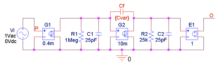
Figure 1. PSpice circuit to plot a fully compensated and a decompensated open-loop gain.
The results from PSpice can be seen in the figure below:
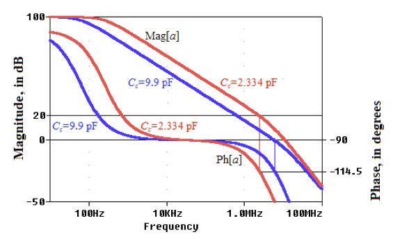
Figure 2. Open-loop gains with full compensation (Cƒ = 9.90 pF for closed-loop gains ≥ 0 dB) and with decompensation (Cƒ = 2.334 pF for closed-loop gains ≥ 20 dB). Both compensations enjoy ɸm ≥ 65.5°
The results elicit the following observations:
- With full compensation (Cƒ = 9.90 pF), the 0-dB gain has the crossover frequency ƒx ≈ 5.86 MHz and the phase margin ɸm = 65.5°. Also, if we configure the fully-compensated op-amp for a 20-dB closed-loop gain, it has ƒx ≈ 633 kHz and ɸm ≈ 87°, an even greater margin than the 0-dB gain.
- With decompensation (Cƒ = 2.334 pF), the 20-dB gain has ƒx ≈ 2.37 MHz (a wider bandwidth than with full compensation) and still ɸm = 65.5°. However, were we to configure the decompensated op-amp for a 0-dB closed-loop gain, it would have ƒx ≈ 11.1 MHz and ɸm ≈ 24°, a poor margin because the decompensated device is meant for gains ≥ 20 dB. With ɸm ≈ 24°, the 20-dB gain would exhibit a peaking of about 7% and a transient response with an overshoot of about 50%, both of which are usually unacceptable.
Now let's move on to considering how we can achieve compensation in our circuit using external factors; for example, resistors.
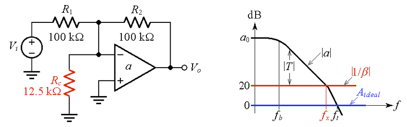
External Compensation Using Resistors
Even though decompensated op-amps are meant for closed-loop gains higher that Amin (Amin = 20 dB in the above example), their superior dynamics makes them attractive also for applications involving gains lower than Amin.
But this would reduce the phase margin ɸm, so it is the user’s responsibility to compensate the circuit externally in order to keep ɸm at the desired level.
To illustrate, let us take the op-amp of Figure 1 in a decompensated form with Cƒ = 2.334 pF, and let us configure it for voltage-follower operation as in Figure 3(a).
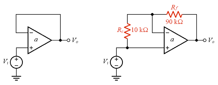
(a) (b)
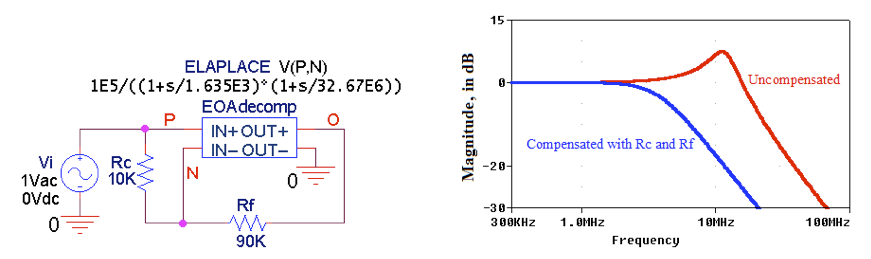
Figure 3. Voltage follower: (a) Uncompensated, and (b) compensated externally for ɸm ≈ 65.5°.
As mentioned, this circuit has a phase margin of only ɸm ≈ 24°. How do we raise it to ɸm = 65.5°? A simple solution is to raise its 1/β curve to 20 dB, while still ensuring unity gain. We achieve this by connecting a resistance pair Rc-Rƒ in a 1-to-9 ratio as shown in Figure 3(b). The closed-loop gain in the idealized limit a → ∞ is still
$$A_{ideal}=1.0V/V$$
Equation 1
(This is the case because for a → ∞ the voltage across the op-amp’s input terminals tends to zero. This implies zero current through Rc and, thus, zero current also through Rƒ. Consequently, the voltage across Rƒ is zero, so we have Vo = Vi.)
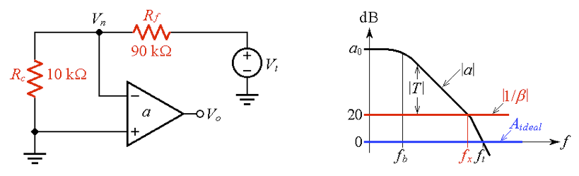
However, the feedback factor β, which we find via the test circuit of Figure 4(a) is
$$β=\frac{V_{n}}{V_{t}}=\frac{R_{c}}{R_{c}+R_{f}}=0.1$$
Equation 2
or 1/β = 10 = 20 dB (note that 1/β ≠ Aideal in this example).
(a) (b)
Figure 4. (a) Circuit to find the feedback factor β of the voltage follower of Figure 3(b), and (b) Bode-plot visualization.
The responses are shown in Figure 5.
(a) (b)
Figure 5. (a) PSpice circuit to visualize (b) the responses of the voltage followers of Figure 3. The Laplace block simulates the decompensated response of Figure 2, obtained with Cƒ = 2.334 pF.
A similar line of reasoning applies to the unity-gain inverting amplifier of Figure 6(a).
(a) (b)
Figure 6. External compensation of a unity-gain inverting amplifier.
In this case, in the limit a → ∞, we have
$$A_{ideal}=-\frac{R_{2}}{R_{1}}=-1.0V/V$$
Equation 3
By inspection, the feedback factor is now
$$β=\frac{R_{1}||R_{c}}{(R_{1}||R_{c})+R_{2}}=0.1$$
Equation 4
In this case, Rc has been chosen so as to make (R1||Rc) = R2/9.
Applications (and Disadvantages) of Resistive Compensation
The above discussion, specialized for the unity-gain noninverting and inverting amplifiers, can easily be generalized to the case of closed-loop gains other than unity, but still such that 1 < (1 + R2/R1) < Amin.
Whether the circuit is used as a noninverting amplifier (Aideal = 1 + R2/R1) or as an inverting amplifier (Aideal = –R2/R1), so long as the condition (1 + R2/R1) < Amin holds, we place a resistance Rc across the op-amp’s input terminals such 1 + R2/(R1||Rc) = 1 + R2/R1 + R2/Rc = Amin.
Resistive compensation, though straightforward, suffers from two disadvantages:
- Any noise that can be modeled with a voltage source in series with the noninverting input, such as the input offset voltage VOS, gets amplified by 1/β, also called the noise gain because of this.
- The loop gain T = (aβ = –Vo/Vt in Figure 4(a)) gets reduced (by a factor of 10 in the present example), causing a drop in the closed-loop DC accuracy of the circuit.
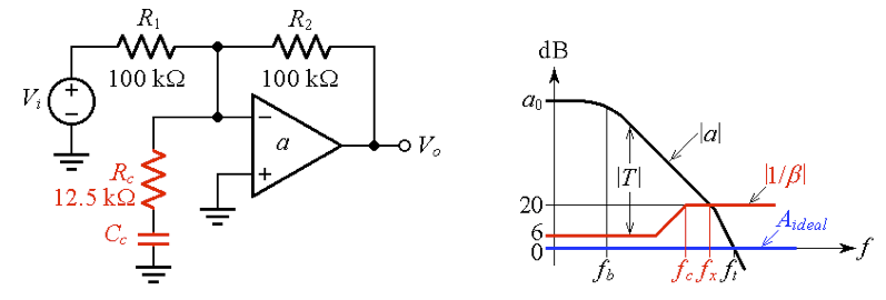
Input-Lag Compensation
We can alleviate the limitations of resistive compensation by placing a suitable capacitance Cc in series with Rc, as depicted in Figure 7(a) for the inverting amplifier.
(a) (b)
Figure 7. (a) Input-lag compensation of the unity gain inverting amplifier, and (b) Bode-plot visualization.
Note that to ensure the desired phase margin, we need to trick the amplifier into the desired rate-of-closure (ROC) only in the vicinity of the crossover frequency ƒx, not necessarily all the way down to DC.
Physically, the 1/β curve breaks at the frequency ƒc at which the capacitive impedance’s magnitude equals Rc, or |1/(j2πCc| = Rc, giving
$$C_{c}=\frac{1}{2πR_{c}f_{c}}$$
Equation 5
To prevent appreciable erosion of the phase margin ɸm, it is customary to place ƒc about a decade below ƒx, or
$$f_{c}≈\frac{f_{x}}{10}$$
Equation 6
For the circuit of Figure 7(a), this implies Cc ≈ 54 pF. The simulation of Figure 8 yields measured values of ƒx = 2.38 MHz and ɸm = 61°.
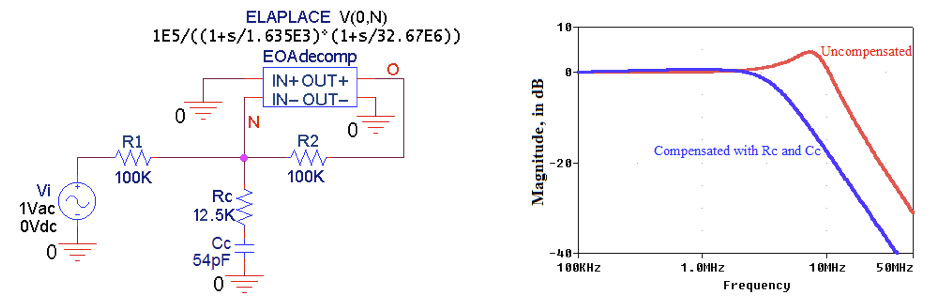
Figure 8. (a) PSpice circuit to (b) visualize the stabilizing effect of input-lag compensation for the unity-gain inverting amplifier.
An Alternative Approach to External Frequency Compensation
Input-lag compensation is notorious for creating a pole-zero doublet in the closed-loop response, which leads, among others, to intolerably long settling time characteristics. These shortcomings are avoided by the alternative compensation approach advanced by Michael Steffes and shown in Figure 9.
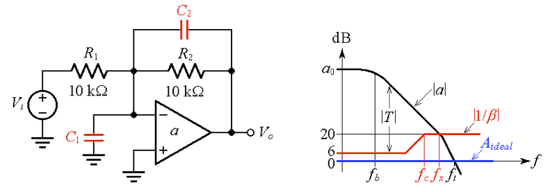
(a) (b)
Figure 9. (a) Michael Steffes’ compensation technique for decompensated op-amps, and (b) Bode plot visualization.
We have already encountered a circuit of this type in a previous article on stray input capacitance compensation, so many of the considerations made there apply also to the present circuit, the only difference being that now C1 is intentional.
We are interested in developing two conditions for specifying the values of C1 and C2. At high frequencies, where the impedances of C1 and C2 are much smaller, in magnitude, than R1 and R2, we can ignore R1 and R2 and state that at high frequencies we have 1/β → 1 + C1/C2.
Imposing 1 + C1/C2 = 20 dB = 10 gives the first condition for our circuit example
$$C_{1}=9C_{2}$$
Equation 7
The second condition stems from the fact that
$$C_{2}=\frac{1}{2πR_{2}f_{c}}$$
Equation 8
so the value of C2 depends on where we decide to position ƒc.
Rather than apply the detailed analysis by Steffes, which is beyond the scope of the present article, here we adopt a heuristic approach.
We start out with Equations (6) and (8), and use the PSpice circuit of Figure 10 to observe the AC responses as we gradually increase ƒc by decreasing C2 while maintaining the condition of Equation (7).
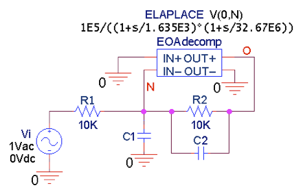
Figure 10. PSpice circuit to plot the AC response of the inverting amplifier of Figure 9a. To plot the transient response, change the AC input source to a pulse source.
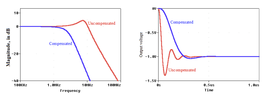
We stop when the AC response just starts to exhibit peaking. This approach gives C2 = 12 pF and C1 = 9C2 = 108 pF, resulting in the well-behaved responses of Figure 11. The AC response has a –3-dB frequency of 2.36 MHz.
(a) (b)
Figure 11. (a) AC response and (b) step response of the inverting amplifier of Figure 10.
It is worth pointing out that any stray capacitance Cn present at the inverting input can be incorporated into this compensation scheme by changing the value of C1 to 9C2 – Cn. So, if, say, Cn = 20 pF, then we use C1 = 88 pF.
In this article, we looked at decompensated and externally compensated operational amplifiers. We used example circuits to demonstrate what op-amp frequency compensation could be achieved through various means and considered each methods pros and cons.
Related Content