 Facebook
 Google
 GitHub
 Linkedin
Frequency Compensation of Operational Amplifiers
Learn about op-amp frequency compensation with an example circuit we'll observe in PSpice.
Learn about op-amp frequency compensation with an example circuit we'll observe in PSpice.
An op-amp is meant to be used in conjunction with an external network connected in such a way as to provide negative feedback. As a signal propagates around the feedback loop, first through the op-amp and then back through the feedback network, it experiences a series of delays, which tend to jeopardize the stability of the circuit.
In fact, if the cumulative effect of these delays results in a phase lag of 180°, feedback turns from negative to positive; moreover, if with positive feedback the overall gain around the loop exceeds unity, the signal will build up in regenerative fashion and result in instability. To prevent this from happening, it is necessary to effect suitable changes in the dynamics of the op-amp, or of the feedback network, or of both, changes that are generally referred to as frequency compensation.
In this article, we'll discuss op-amp frequency compensation and its importance in circuit stability.
Op-Amp Frequency Compensation
Nowadays most op-amps come compensated internally by means of suitable on-chip components. Typically, the compensation is intended for closed-loop gains all the way down to the unity gain of voltage-follower operation. A subclass of op-amps come compensated for closed-loop gains above a value greater than unity, such as 10 V/V. Called decompensated op-amps, they offer faster dynamics than if they had been compensated for unity-gain. (We will cover this concept in more depth in a future article.)
If the feedback network contains reactive elements, whether intentional or parasitic, the stability of the circuit may suffer, in which case it is the responsibility of the user to suitably modify the dynamics of the feedback network so as to ensure the desired degree of stability. Familiar examples of destabilizing situations are provided by capacitive loads, stray input capacitances, and composite amplifiers, the latter being characterized by the fact that the feedback network itself comprises another op-amp.
Internal Compensation of an Operational Amplifier: An Example Circuit
Even though the user has no control over internal compensation, it pays to possess a basic understanding of internal compensation for a more effective application of op-amps.
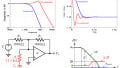
Great many op-amps consist of (1) an input stage to provide differential gain, (2) an intermediate stage to provide additional gain, and (3) an output stage to provide power drive. The transistors and the stray capacitances of the nodes along the signal path of each stage create delays that we lump together and model with a low-pass R-C network, as depicted in Figure 1. (For simplicity, we will ignore the delays of the output stage because it is usually much faster; in on-chip systems not requiring power drive, this stage is often omitted altogether.)
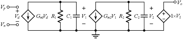
Figure 1. Approximate AC model of an op-amp.
We wish to investigate the op-amp’s overall gain, a = Vo/Vd, also known as the open-loop gain. At DC, where all capacitors act as open-circuits, the gain a takes on the value
$$a_{0}=G_{m1}R_{1}\times G_{m2}R_{2}\times1=G_{m1}R_{1}G_{m2}R_{2}$$
Equation 1
In AC operation, the circuit presents two pole frequencies,
$$f_{1}=\frac{1}{2πR_{1}C_{1}}$$ $$f_{2}=\frac{1}{2πR_{2}C_{2}}$$
Equation 2
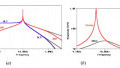
Let us now enlist PSpice to observe this amplifier in feedback operation. With the component values of Figure 2, Equations (1) and (2) give a0 = 400×250 = 105 V/V = 100 dB, ƒ1 = 6.366 kHz, and ƒ2 = 254.6 kHz.
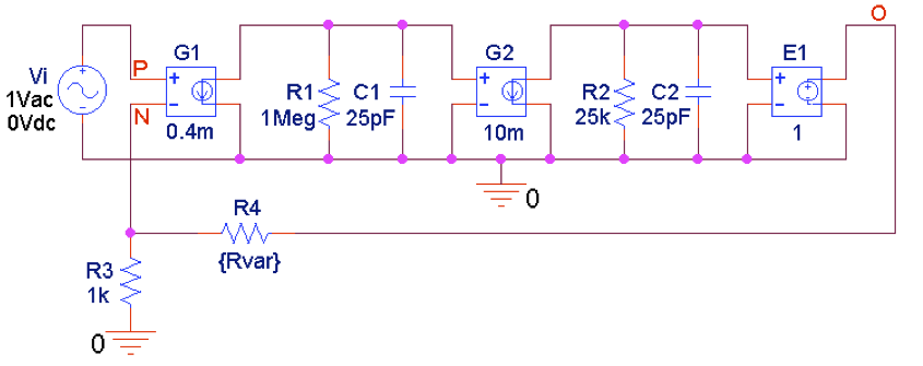
Figure 2. PSpice circuit to plot closed-loop gains in 20-dB steps determined by R4.
Connecting the voltage divider R3-R4 between the output node and the inverting input node establishes negative-feedback operation with a feedback factor β of
$$β=\frac{R_{3}}{R_{3}+R_{4}}$$
Equation 3
and configures the circuit as a noninverting amplifier whose closed-loop gain Vo/Vi is, ideally
$$A_{ideal}=\frac{1}{\beta}=1+\frac{R_{4}}{R_{3}}$$
Equation 4
Stepping R4 through the values of 0, 9 kΩ, 99 kΩ, 999 kΩ, and 9,999kΩ yields the family of closed-loop plots of Figure 3 (also shown for convenience is the plot of the open-loop gain a).
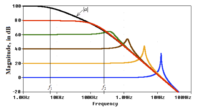
Figure 3. Closed-loop gains of the circuit of Figure 2 for different amounts of feedback.
We observe that for large values of Aideal, the AC responses are reasonably flat, but for lower values of Aideal, there is an increasing amount of peaking. We justify this by noting that since 1/β = Aideal, lowering Aideal means lowering the 1/β curve and thus shifting the crossover frequency towards regions of the steeper slope of the |a| curve.
The resulting increase in the rate-of-closure (ROC) reduces the phase margin of the circuit, thus inviting instability. (Having only two poles, our circuit will not oscillate, though it will exhibit intolerable peaking and ringing at low gains; however, the presence of additional high-frequency poles, not accounted for in our simplified op-amp model, is likely to cause the circuit to oscillate).
It is apparent that the configuration most prone to oscillation is the unity-gain voltage follower, for which β = 1. If the op-amp is compensated for an adequate phase margin for unity-gain operation, then it will be stable also for all other closed-loop gains.
Dominant-Pole Compensation
Among all the closed-loop gains of Figure 3, the highest gain (80 dB) has the best profile because of the absence of peaking. This is because its crossover frequency occurs about halfway between ƒ1 and ƒ2, where the rate-of-closure (ROC) is about 20 dB/dec, so the phase margin is about 90°.
We want also all other gains to enjoy a similar phase margin, all the way down to unity-gain. This requires that the |a| curve exhibit a slope of –20 dB/dec throughout. The open-loop gain a must, therefore, be modified so that its profile is dominated by a single pole.
In the next article, we will discuss one method of achieving this via shunt capacitance.
In this article, we went over op-amp frequency compensation and considered an example circuit in PSpice. In the next article, we'll look at a method of achieving compensation via shunt capacitance.
Related Content


I loved the way an operational amplifier was modeled! It gave me a good insight into why more than one pole might be present in an operational amplifier!
Huh?