Facebook
 Google
 GitHub
 Linkedin
Integrator Limitations: Active Phase-Error Compensation
In this article, we will discuss active phase-error compensation and how it can prevent Q enhancement.
A popular application of integrators is in the synthesis of dual-loop integrator filters, such as the state-variable and the biquad types. The integrators are usually implemented with constant gain-bandwidth-product (constant GBP) op-amps. We are about to see that the ensuing phase error causes an undesirable increase in the Q-factor of dual-integrator filters. Called Q enhancement, not only does it prevent the user from meeting the desired filter specifications, but it also tends to destabilize the circuit.
Mercifully, we can prevent the Q enhancement via active phase-error compensation. Before proceeding, we recall that integrator behavior is affected also by the op-amp’s output impedance zo, which causes signal feedthrough around the op-amp. In the following we assume |zo| to be so much smaller than the integrator’s resistance R, that feed-through can be ignored.
State-Variable Filters
Figure 1 shows one of several incarnations of the state-variable filter (SVF).
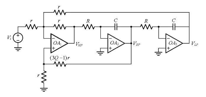
Figure 1. State-variable filter of the KHN type.
Also called the KHN type for its inventors W. J. Kerwin, L. P. Huelsman, and R. W. Newcomb, who first reported it in 1967, it provides the second-order high-pass, band-pass, and low-pass responses simultaneously. For this reason, the SVF is also referred to as a universal filter.
Figure 2 shows the PSpice circuit of a SVF that has been designed for f0 = 10.0 kHz and Q = 25.
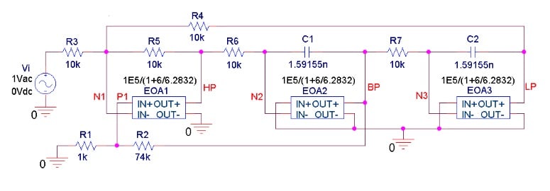
Figure 2. PSpice circuit of an SVF filter designed for f0 = 10.0 kHz and Q = 25. The circuit uses Laplace blocks to simulate op-amps with GBP = 1 MHz.
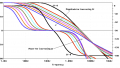
According to the plots of Figure 3(a), the three responses seem to conform to their ideal counterparts up to about 100 kHz, at which point they begin to acquire an additional slope of –20-dB/dec because of the transition frequency ft = 1 MHz of the op-amps.

Figure 3. (a) High-pass (HP), band-pass (BP), and low-pass (LP) responses of the PSpice circuit of Figure 2. (b) Expanded view of the band-pass (BP) response, showing Q enhancement as well as a downshift in the resonant frequency. The ideal responses are shown in gray.
However, a look at the expanded BP view of Figure 3(b), reveals two discrepancies from the ideal:
- The resonant frequency is downshifted from the design value of f0 = 10.0 kHz. This stems from the magnitude error of the individual integrators.
- The peak gain, which for the KRN circuit coincides with the Q-factor of the filter itself, undergoes a dramatic increase above the design value of 25. Should the Q-factor reach infinity, the circuit would become oscillatory. Q enhancement stems from the phase error of the integrators.
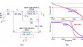
Figure 4 shows how to actively compensate the KHN filter of Figure 2.
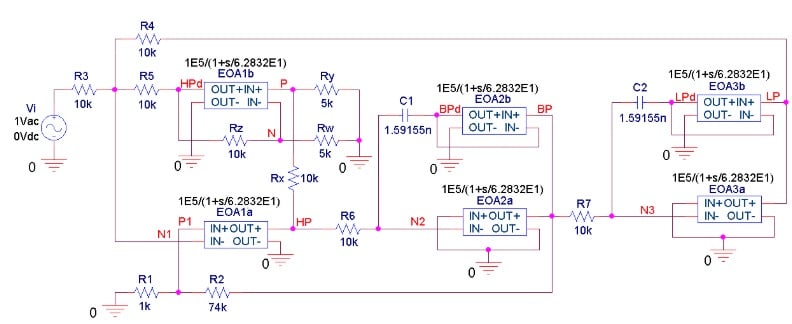
Figure 4. Active phase-error compensation for the circuit of Figure 2 to prevent Q enhancement.
We compensate the integrating op-amps EOA2a and EOA3a by means of the unity-gain voltage followers EOA2b and EOA3b, respectively. Likewise, we compensate the summer op-amp EOA1a with a unity-gain stage having the same closed-loop pole frequency as EOA1a itself. Now, the noise gain of OA1a is 1 + R5/(R3||R4) = 3, so its closed-loop pole frequency is ft /3 = 333.3 kHz.
To mimic this frequency, the compensating op-amp EOA1b uses Rz and Rw to establish a noise gain of 1 + Rz/Rw = 3. However, this will also force EOA1b to amplify by 3, so we interpose the voltage divider Rx-Ry to drop the overall gain HPd/HP from 3 to 1.
The beneficial effect of active compensation is evidenced in Figure 5, where it is seen that the effective Q-factor, in excess of 100 in the uncompensated case, has been restored to its intended value of 25.
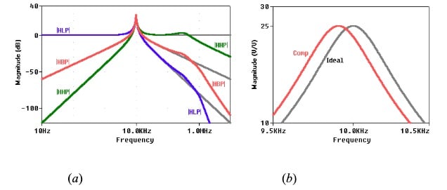
Figure 5. (a) The HP, BP, and LP responses of the PSpice circuit of Figure 4. (b) Expanded view of the BP response, showing the disappearance of Q enhancement. The ideal responses are shown in gray.
The filter still suffers from a frequency downshift of about 1%, but we can readily compensate for this by reducing both C1 and C2 by about 1%, while leaving R6 and R7 unchanged, or vice versa.
Doubling the op-amp count from 3 to 6 might seem like overkill, but nowadays, with matched op-amps available both as duals and as quads at little or no extra cost, a compensated SVF is quite realistic, given the advantage of having all three responses (HP, BP, and LP) available simultaneously.
Biquad Filters
Like the SVF just discussed, the circuit of Figure 6, also known as the Tow-Thomas filter, comprises two integrators.
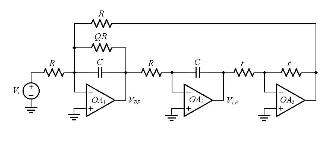
Figure 6. Biquad filter.
The combination of the inverting integrator OA2 and the unity-gain-inverting amplifier OA3 acts as a noninverting integrator. OA1 operates as a summing lossy integrator: it sums the input Vi and the noninverting integrator’s output, and it provides lossy integration due to the presence of the feedback resistance QR, whose task is to control the Q-factor. (Leaving this resistor out would result in an infinite Q and most likely cause the circuit to oscillate.)
Figure 7 shows the PSpice circuit of a biquad filter that has been designed for f0 = 10.0 kHz and Q = 25.
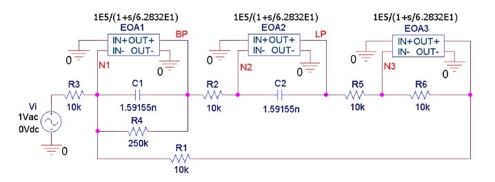
Figure 7. PSpice circuit of a biquad filter designed for f0 = 10.0 kHz and Q = 25, using op-amps with GBP = 1 MHz.
According to the plots of Figure 8(a), the two responses seem to conform to their ideal counterparts up to about 100 kHz, at which point they begin to acquire an additional slope of –20-dB/dec because of the transition frequency ft = 1 MHz of the op-amps.
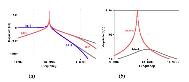
Figure 8. (a) BP and LP responses of the PSpice circuit of Figure 7. (b) Expanded view of the BP response, showing Q enhancement as well as a downshift in the resonant frequency. The ideal responses are shown in gray.
However, a look at the expanded BP view of Figure 8(b) reveals two discrepancies from the ideal:
- The resonant frequency is downshifted from the design value of f0 = 10.0 kHz. This stems from the magnitude error of the individual integrators.
- The peak gain, which for the biquad filter coincides with the Q-factor of the filter itself, undergoes a dramatic increase above the design value of 25. With its Q-factor in excess of 1000, the circuit is about to oscillate. Q enhancement stems from the phase error of the integrators.
Figure 9 shows a simple rewiring of the circuit that will prevent Q enhancement.
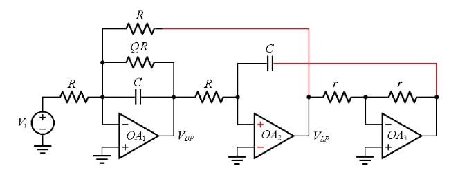
Figure 9. Rewiring the biquad filter of Figure 6 to prevent Q enhancement.
Recall that in the vicinity of f0 the integrator OA1 yields a phase error of
\[\epsilon_\phi \cong -f/f_t\]
Equation 1
The integrator OA2, rewired with the unity-gain inverting amplifier OA3 now placed inside its feedback loop, and with OA2’s inputs swapped, yields a phase error of
\[\epsilon_\phi \cong + f/f_t\]
Equation 2
The two phase errors tend to cancel each other out, creating the appearance of a net phase error of zero, and thus preventing Q enhancement.
Figure 10 shows the PSpice circuit of our rewired filter.
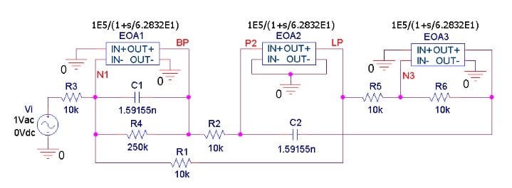
Figure 10. PSpice circuit of the actively-compensated biquad filter of Figure 7.
The plots of Figure 11 confirm the absence of Q enhancement.
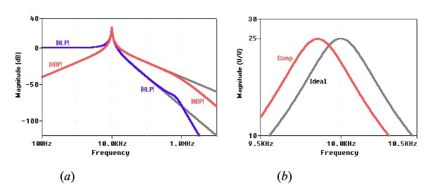
Figure 11. (a) The BP and LP responses of the PSpice circuit of Figure 10. (b) Expanded view of the BP response, showing the disappearance of Q enhancement. The ideal responses are shown in gray.
However, the resonant frequency of the compensated response is downshifted from 10.0 kHz to 9.8524 kHz. Lowering C1 and C2 to 1.5679 nF will center the resonant frequency at 10.0 kHz.
Conclusion
We summarize our four-article series on integrators as follows:
- The best frequency range for an integrator is from the pole frequency fb of the op-amp’s open-loop gain to the unity-gain frequency f0 of the integrator. This is the range over which both the magnitude and phase errors are at a minimum.
- Once the value of f0 has been decided, the integrator designer should select an op-amp with a transition frequency ft such that ft >> f0.
- At high frequencies, integrator behavior is affected also by the op-amp’s output impedance zo. To minimize the impact of zo, the designer should select an op-amp such |zo| << R at the upper frequency region of interest, where R is the resistance that, together with C, sets f0 . Alternatively, once an op-amp with a given |zo| is selected, the designer should specify R such that R >> |zo|.
- The magnitude error causes a downshift of the integrator’s actual unity-gain frequency from the design value of f0. This can be compensated for by suitably predistorting the value of R or of C.
- The phase error tends to destabilize dual-integrator filters such as the state-variable and the biquad types. This form of degradation, referred to as Q enhancement, can be prevented via active phase-error compensation.
- Our analysis has stipulated op-amp open-loop responses containing a single pole. However, practical open-loop responses contain additional poles (and possibly zeros) above ft, which tend to further increase the magnitude and phase errors somewhat. Also, the stray capacitance at the inverting-input of an integrator tends to play some role in the deviation from the ideal. Consequently, the results of our derivations should be taken as starting points that may require a certain amount of additional tweaking.
Related Content